
A significant part of this work will be devoted to reliability studies of next-generation 2D FETs. Since so far no reliability theory has been developed for these new technologies, we will start by using general models previously developed for Si MOSFETs. Hence, in this chapter a brief background of the main reliability issues in Si technologies and their modeling will be provided.
Understanding of reliability models requires basic knowledge on the main reliability issues observable in modern Si MOSFETs. The related information will be provided in this section.
Negative bias-temperature instability (NBTI) is one of the most crucial degradation mechanisms observed in modern CMOS devices. Pure NBTI degradation typically occurs if the device is examined at high enough temperatures and if considerable negative gate voltages are applied when the source and drain terminals are grounded. While leading to a shift of the threshold voltage and variation of the subthreshold swing, NBTI may significantly impact device performance. If the device operates in extrem working conditions1, the impact of NBTI can be very strong. However, when the stress is removed, the device parameters tend to return back to their initial values, i.e. NBTI degradation is recoverable. During the last decade investigation of NBTI has attracted a considerable amount of attention [89, 59, 80, 60, 65, 66, 79, 76, 7, 58]. One of the main reasons for this is the agressive scaling of the devices, which requires the use of thinner gate oxides, thereby leading to larger oxide fields.
The impact of NBTI on the device characteristics is associated with the trapping of carriers by oxide traps [173, 63] (e.g. E’ centers and switching oxide traps), which can exchange charges with the channel, and interface states [61] (e.g. Pb centers). The positive charge variation associated with oxide traps is
|
| (3.1) |
where fox(x, Et, t) is the occupancy of oxide traps, ΔDox(x, Et, t) is the density of states in the oxide and dox is the oxide thickness. Since oxide traps are located in the oxide bulk and have larger time constants, their occupancy can not follow the Fermi level. Conversely, the charging and discharging of interface states is very fast. Hence, the captured variation of positive charge follows the Fermi level EF and can be given by
 | (3.2) |
where fit(EF, Et, t) is the occupancy of interface states and ΔDit(Et, t) the time-dependent density.
The strongest impact of NBTI is observed for p-MOSFETs, which typically operate at negative gate voltages. However, some NBTI degradation, although less significant, can be observed for n-MOSFETs [34, 80] (in that case negative gate voltage corresponds to the accumulation region).
Positive bias-temperature instability (PBTI) is a counterpart of NBTI which occurs at positive gate voltages. Although this degradation issue is expected to impact n-MOSFETs, it has already been shown in [34, 80] that for SiON devices threshold voltage shifts induced by PBTI in n-MOSFETs can be several orders of magnitude smaller than NBTI shifts in p-MOSFETs. Moreover, they are even smaller than PBTI shifts in p-MOSFETs, which correspond to accumulation stress voltage and hence are not of any practical interest. Therefore, investigation of PBTI in Si MOSFETs with SiON insulators is much less intensive compared to NBTI studies. However, PBTI is often reported to be a serious reliability issue in Si MOSFETs with high-k gate insulators[75, 175]. Furthermore, it will be shown that this degradation issue can be very crucial in next-generation 2D FETs.
Hot-carrier degradation (HCD) is a reliability issue which takes place if a non-zero voltage is applied at the drain. Since most device operation conditions assume some voltage applied at the gate, HCD typically occurs in conjuction with NBTI or PBTI [1].
HCD is associated with defects situated closely to the channel/oxide interface and becomes more pronounced for larger drain voltages. During device operation this interface is bombarded by highly-energetic (i.e. “hot”) carriers, which leads to a rupture of hydrogene (Si-H) bonds and the formation of dangling bonds, i.e. interface states [1, 172, 171]. These interface states are inhomogeneously distributed along the channel with a maximum density in the proximity of the drain [171, 16]. The latter occurs because the electric field near the drain is largest, making carrier energies higher.
Trapping of carriers by interface states created by HCD leads to a shift of the threshold voltage. On the other hand side, scattering of carriers on charged interface states reduces transconductance and mobility. However, contrary to NBTI and PBTI, HCD in Si MOSFETs is typically non-recoverable, since only a strong permanent component associated with a number of dangling bonds is present.2
Other reliability issues which are typically observed in Si MOSFETs are time-dependent dielectric breakdown (TDDB), random telegraph noise (RTN) and 1/f noise. However, they will not be studied in the course of this work.
TDDB is a degradation mechanism which leads to the failure of the gate dielectric resulting from operation for a long time [155, 156].3 Obviously, in real device operation conditions, TDDB usually acts in conjuction with BTI and/or HCD.
RTN is observed in extremely scaled devices, where the capture and emission of carriers by individual traps results in a discrete modulation of the drain current at fixed drain or gate voltage. Contributions of multiple traps may lead to a multi-level RTN [78]. However, this is not an issue for large devices with a great number of defects.
1/f noise (or flicker noise) is the counterpart of RTN which is characterized by a continuous spectral density behaving as 1 over frequency (1/f) [154, 186]. Contrary to RTN, it can be observed in large area devices.
In this section we will provide information on general models which are employed to describe BTI degradation/recovery dynamics in Si MOSFETs. In the following chapters these models will be adjusted to characterize the reliability of next-generation 2D FETs.
The universal relaxation model [61, 64] has been derived for fitting of NBTI degradation/recovery in Si technologies. In order to distinguish between the degradation during the stress and relaxation phases, the authors of [61] operate with the degradation magnitude accumulated during the stress S0(ts) and relaxation magnitude R0(ts, tr). It is assumed that the relaxation starts as soon as the stress voltage is removed. Hence, the relaxation magnitude is treated as a function of both stress time ts and relaxation time tr = t - ts.
However, most experimental techniques typically introduce some measurement delay tM between the end of the stress and the beginning of recovery observation. Since the recovery of NBTI degradation starts faster than microseconds after the BTI stress is removed [146], some fraction of recovery is lost.4 Hence, one has to operate with RM(ts) = R0(ts, tM) and SM(ts) = S0(ts, tM) [61] when normalizing the obtained recovery data by the first measurement point. Also, a fractional recovery rf(ts, tr) = R0(ts, tr)/RM(ts) can be introduced [146, 61].
According to [33], the normalized NBTI recovery obtained using different stress times has the same dependence on the normalized relaxation time ξ = tr∕ts. However, the recovery of NBTI is typically not complete, and has some permanent component P(ts) = S0(ts) - R0(ts, 0) [143, 62, 58]. Therefore, in the spirit of [33] and taking into account the permanent component, the authors of [61] have introduced a general universal relaxation function, which is given by
 | (3.3) |
After a number of attempts have been made to empirically find the exact form of universal relaxation function [2, 169, 170], in [61] it has been demonstrated that the one suitable for the whole spectra of experimental data available for NBTI is
 | (3.4) |
where B and β are the fitting parameters which have to be adjusted for each particular case5, while rf(ts, tr) = r(ξ)/r(ξM) with ξM = tM∕ts. Equation 3.4 can be successfully applied to fit normalized NBTI recovery in Si technologies and also to predict time to failure of the device. However, one should note that in [61] equation 3.4 has been empirically derived assuming a zero permanent component. At the same time, according to equation 3.3, P(ts) has to be subtracted from the experimental data before analyzing universality.
Another important consequence following from the universal relaxation model is that it allows for the extrapolation of the degradation magnitude at a zero measurement delay. While the degradation magnitude is expected to follow a power law S0(ts) = Atsn, in [61] it has been shown that experimentally observed threshold voltage shifts measured at t = t M can be expressed by
 | (3.5) |
with B and β given by equation 3.4. This expression allows to combine experimental data measured with different delays tM.
One should note that although the universal relaxation model was originally developed for NBTI in p-MOSFETs, in [64] it was also found to be suitable for capturing both NBTI and PBTI in p- and n-MOSFETs.
The capture/emission time (CET) map model [69] assumes that BTI is due to both interface states and oxide traps which can exchange charges with the channel. Each of these defects is assumed to have two stable states, i.e. charged and neutral. The charge exchange events between different states are treated as first-order non-radiative multiphonon (NMP) processes [66] with the capture and emission times given by
 | (3.6) |
 | (3.7) |
Here τ0 is the effective time constant which weakly depends on BTI stress conditions, and Ec and Ee are capture and emission energy barriers, respectively.
In the CET map model, BTI is assumed to be the collective response of different oxide traps and interface states, while capture and emission are considered as thermally activated processes [66, 147]. Hence, the distributions of Ec and Ee are employed to obtain CET maps using equations 3.6–3.7. This allows to avoid direct modeling of widely distributed time constants τc and τe and also leads to a built-in temperature dependence of the model. At the same time, the dependence on stress voltage has to be introduced by adjusting model parameters [69].
Initially, the CET maps were extracted numerically by differentiating the obtained recovery traces for threshold voltage shift [147]. The analysis of the results obtained at different temperatures has shown that the capture and emission times are correlated. Namely, a decrease of the emission time at higher temperature leads to a reduced capture time [96] and vice versa. Therefore, it was suggested to express this correlation by linking the activation energies of capture and emission processes as Ee = Ec + ΔEe, with ΔEe being an uncorrelated part of Ee. Since many experimental features of BTI degradation/recovery dynamics could be captured by a Gaussian distribution, the authors of [69] assume that the quantities Ee, Ec and ΔEe are normally distributed with the mean values μe, μc and μΔe, and standard deviations σe, σc and σΔe, respectively. This allows for the constructing of a bivariate Gaussian distribution, which is given by
 | (3.8) |
Obviously, the marginal distributions g(Ee) and g(Ec) can be obtained by integrating g(Ec, Ee) over Ec and Ee, respectively. At the same time, the main parameters of g(Ee) can be expressed by μe = μc + μΔe and σe2=σ c2+σ Δe2.6
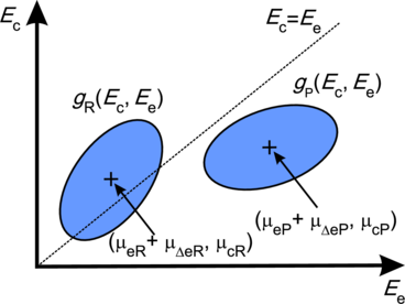
However, fitting of the BTI recovery in Si technologies typically requires two bivariate Gaussian distributions given by equation 3.8. As shown in Figure 3.1, one (gR(Ec, Ee)) is necessary to express the contribution of the recoverable component and the other is used for the permanent component (gP(Ec, Ee)). Typically, the mean values and standard deviations for these two distributions are different, i.e. one has to operate with μcR, μcP, σcR, σcP and so on.
Taking into account equations 3.6– 3.7, which link the time constants with corresponding activation energies, bivariate Gaussian distributions of Ec and Ee can be used to calculate the CET map. Obviously, this CET map will present nothing else than a combination of two bivariate Gaussian distributions for τc and τe. Hence, the threshold voltage shift can be obtained by integrating these distributions over all defects with τc < ts and τe > tr, and reads
 | (3.9) |
where AR and AP are the fitting parameters which express the magnitudes of the contributions associated with the recoverable and permanent components, respectively.
However, in some cases it is more convenient to integrate the original distributions obtained for the activation energies. Thus the equation 3.9 can be rewritten as
 | (3.10) |
where aR∣P and bR∣P are obtained by recalculating the integration limits using equations 3.6– 3.7 and given by
 | (3.11) |
 | (3.12) |
In general, integration in equations 3.9– 3.10 has to be done numerically. However, in [69] one can find an analytical approximation.
According to the description above, the CET map model allows for the simulation of ΔV th(tr) recovery traces for different stress times. Hence, by adjusting the distribution widths and positions (i.e. mean values and standard deviations) one can approximate the measured BTI recovery. Moreover, extrapolation of ΔV th at zero measurement delay is possible, similarly to the universal relaxation model. However, a significant advance of the CET map model compared to the universal relaxation model is that the former incorporates a temperature dependence, which results in more stable fits.
The models described above allow for the fitting of a wide range of NBTI and PBTI stress/recovery characteristics. However, they are not always consistent with a number of features which have been extracted from TDDS measurements when characterizing single defects. The most important of them is associated with significant differences in emission times for the defects with similar capture times as well as bias dependence of emission times for some defects. Hence, a more general four-state NMP model was derived in [66].
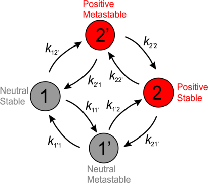
The four-state NMP model considers interaction of a single carrier with an individual defect. Contrary to the two-state CET map model, this defect is assumed to have four different states. Namely, both neutral and charged configurations of the defect are characterized by one stable and one metastable state. In Figure 3.2 this situation is illustrated for the case of hole trapping. One can see that there are eight different transitions which may occur. While all the transitions between stable and metastable states of one configuration (11’, 22’, 1’1 and 2’2) are associated with structural relaxation of the defect, transitions between the states with different configurations (12’, 2’1, 1’2, 21’) correspond to a charge exchange between the defect and the device channel. Also, each of these transitions is described by a certain transition rate kij. These transition rates are calculated by assuming that the defect time dynamics can be described using a continuous-time Markov process X(t) [55], i.e. the defect can only be in one state at a certain point in time. Hence, the probability of finding the defect in a certain state pi(t) = P{X(t) = i} and Σipi(t) = 1, where i = 1, 1′, 2, 2′. Following the theory of Markov processes described in [55], the authors of [66] derived a master equation for all four probabilities pi(t), which reads
 | (3.13) |
The rates for each of the transitions marked in Figure 3.2 can be calculated using NMP theory7. It has been found that the transition rates for the transitions between stable states and metastable states of opposite configurations depend on the applied gate voltage and can be given by
 | (3.14) |
 | (3.15) |
 | (3.16) |
 | (3.17) |
Furthermore, the transitions between stable and metastable states of one configuration are only activated by temperature and can be written as8
 | (3.18) |
 | (3.19) |
 | (3.20) |
 | (3.21) |
Here σp is a hole capture cross-section, v0 ≈1013s-1 is the attempt frequency [56], and p and v tp are hole concentration and thermal velocity, respectively9. The trap levels in neutral stable and metastable states are given by ET and ET′, while ε ij are the activation barriers. The configuration of these parameters is shown in Figure 3.3, where the adiabatic potentials for different states of the defect are plotted versus the reaction coordinate z.
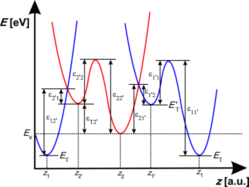
The bias dependent barriers ε12′ and ε1′2 are calculated by quadratic expansion of the adiabatic potentials around the minima corresponding to different states (zi), while the other barriers are obtained as explicit parameters [66]. Then the calculated transition rates can be used to express individual contributions of each defect state to the time constants [66].
Although originally the four-state NMP model was developed to capture the experimental features of single defects observed in TDDS data, its complexity allows for a reliable description of a wide spectrum of effects related to the trapping of carriers in the device channel. Hence, PBTI and NBTI can be properly modeled using this approach. Also, a major advantage of the four-state NMP model compared to the CET map model and other previously used approaches is that it can be coupled with DD simulations. This allows its implementation into professional simulation software and makes the four-state NMP model potentially suitable for the simulations of next-generation 2D FETs reliability. Although a number of further efforts still have to be undertaken to adjust this model to 2D channel geometries, in this work the validity of this approach will be illustrated on an example of MoS2 FETs.
It should be noted that although in Si technologies modeling of HCD requires a separate description10, we assume that in 2D technologies the absence of dangling bonds makes BTI and HCD more similar. Therefore, according to our current understanding, the models derived for BTI in Si MOSFETs, after some adjusting, should be suitable to capture the dynamics of both BTI and HCD in 2D FETs. Especially valuable in this context is the four-state NMP model.