For the electronic structure calculations, the Hamiltonian of the GNRs is described in the standard first nearest-neighbor atomistic tight-binding ![]() orbital approximation. The hopping parameter is set to
orbital approximation. The hopping parameter is set to
![]() and the on site potential is shifted to zero so
that the Fermi level remains at
and the on site potential is shifted to zero so
that the Fermi level remains at
![]() . This model has been
recently used to describe the electronic transport of ELD-ZGNR with
double-vacancies and the results are in good agreement with
first-principle calculations and experimental
studies [89,90]. To date, only
a few first-principle calculations and experimental studies have been
conducted for structures that include ELDs [91,92,90]. The two main features of the electronic structure, the asymmetry between electrons and holes,
and the metallic behavior of the ELD in the graphene ribbon have been described in these studies, and are also captured by the
tight-binding model, which is used here for ZGNR-based structures.
. This model has been
recently used to describe the electronic transport of ELD-ZGNR with
double-vacancies and the results are in good agreement with
first-principle calculations and experimental
studies [89,90]. To date, only
a few first-principle calculations and experimental studies have been
conducted for structures that include ELDs [91,92,90]. The two main features of the electronic structure, the asymmetry between electrons and holes,
and the metallic behavior of the ELD in the graphene ribbon have been described in these studies, and are also captured by the
tight-binding model, which is used here for ZGNR-based structures.
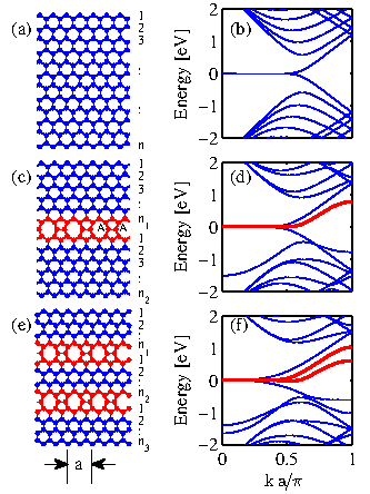
The changes in the electronic structure of the ZGNRs after the
introduction of the ELD are demonstrated in
Fig. 3.19. Figure 3.19-a shows
the atomistic geometry of the pristine ZGNR of width
![]() (with 20 zigzag edge lines) and
Fig. 3.19-b its electronic structure. The Fermi
level is at
(with 20 zigzag edge lines) and
Fig. 3.19-b its electronic structure. The Fermi
level is at
![]() due to the symmetry of the electron and
hole bands. Figure 3.19-c shows the structure of
the ELD-ZGNR with the same width. The region where the ELD is
introduced is shown in red color. The ELD changes the hexagons of the
GNR to pentagons and octagons after a local rearrangement of the
bonding and the introduction of two additional atoms in the unit cell.
To describe the ELD-ZGNR structure a two parameter notation is used as ELD-ZGNR(
due to the symmetry of the electron and
hole bands. Figure 3.19-c shows the structure of
the ELD-ZGNR with the same width. The region where the ELD is
introduced is shown in red color. The ELD changes the hexagons of the
GNR to pentagons and octagons after a local rearrangement of the
bonding and the introduction of two additional atoms in the unit cell.
To describe the ELD-ZGNR structure a two parameter notation is used as ELD-ZGNR(![]() ,
,![]() ), where
), where ![]() and
and ![]() are the indices of the partial-ZGNRs above and below the line defect,
respectively (i.e. the number of zigzag edge lines of atoms). In this work we only consider the cases
are the indices of the partial-ZGNRs above and below the line defect,
respectively (i.e. the number of zigzag edge lines of atoms). In this work we only consider the cases ![]() .
.
|
The bandstructure of the
ELD-ZGNR(10,10) is shown in Fig. 3.19-d. The
thick-red line shows a new band that is introduced in the conduction
band near the Fermi energy (
![]() ), which corresponds to
the ELD. There are two effects that result in the creation of the extra
band. Part of the physics behind this is explained by Pereira et
al. in Ref. [93]. The first effect is that a defect in the
graphene system will introduce states that reside close to the Fermi
level at
), which corresponds to
the ELD. There are two effects that result in the creation of the extra
band. Part of the physics behind this is explained by Pereira et
al. in Ref. [93]. The first effect is that a defect in the
graphene system will introduce states that reside close to the Fermi
level at
![]() . This is similar to the edge states of the
ribbons that tend to reside near the Fermi level. The second effect
again described in Ref. [93], is that an asymmetry in the
dispersion between electrons and holes will be created when carbon
atoms of the graphene sublattice A (or B) are coupled with
atoms from A (or B) again. Usually, the atomic arrangement in
graphene can be splitted in sublattices A and B, where atoms
from A couple to B and vise versa. When this happens, the
dispersion is symmetric in the first-nearest neighbor tight-binding model. At a
defect site such as the ELD, where A connects to A
as seen in Fig. 3.19-c, such asymmetry can be
observed. The fact that the overall bandstructure has additional bands
compared to the pristine ribbon is also caused by the two extra
atoms in the unit cell.
. This is similar to the edge states of the
ribbons that tend to reside near the Fermi level. The second effect
again described in Ref. [93], is that an asymmetry in the
dispersion between electrons and holes will be created when carbon
atoms of the graphene sublattice A (or B) are coupled with
atoms from A (or B) again. Usually, the atomic arrangement in
graphene can be splitted in sublattices A and B, where atoms
from A couple to B and vise versa. When this happens, the
dispersion is symmetric in the first-nearest neighbor tight-binding model. At a
defect site such as the ELD, where A connects to A
as seen in Fig. 3.19-c, such asymmetry can be
observed. The fact that the overall bandstructure has additional bands
compared to the pristine ribbon is also caused by the two extra
atoms in the unit cell.
Moving one step further, in Fig. 3.19-e the geometry of a
GNR with two ELDs is shown. This structure is denoted as
2ELD-ZGNR(![]() ,
,![]() ,
,![]() ), where
), where ![]() ,
, ![]() , and
, and ![]() denote the
the number of zigzag carbon lines above, within, and below the line
defects. Figure 3.19-f shows the electronic
structure of the 2ELD-ZGNR(8,4,8). In this case two additional bands
are introduced near the Fermi level as designated by the thick-red
lines. In this structure the asymmetry between electron and hole bands
around the Fermi level (
denote the
the number of zigzag carbon lines above, within, and below the line
defects. Figure 3.19-f shows the electronic
structure of the 2ELD-ZGNR(8,4,8). In this case two additional bands
are introduced near the Fermi level as designated by the thick-red
lines. In this structure the asymmetry between electron and hole bands
around the Fermi level (
![]() ) is further enhanced.
) is further enhanced.
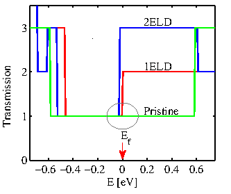
Figure 3.20 demonstrates the increase in the asymmetry of
the bands around the Fermi level by showing how the transmission
changes when one or two ELDs are introduced in the
channel. For the pristine ZGNR, the transmission is equal to one,
indicating the existence of a single propagating band at energies
around the Fermi level (green line). With the introduction of one ELD,
the conduction band (
![]() ) is composed of two subbands,
whereas the valence band (
) is composed of two subbands,
whereas the valence band (
![]() ) is still composed of one
subband. With the introduction of two ELDs, three conduction subbands
appear, but still only one valence subband. As it
will be shown below, this asymmetry will improve the Seebeck
coefficient. This constitutes the first design step in improving the
thermoelectric performance of ZGNRs.
) is still composed of one
subband. With the introduction of two ELDs, three conduction subbands
appear, but still only one valence subband. As it
will be shown below, this asymmetry will improve the Seebeck
coefficient. This constitutes the first design step in improving the
thermoelectric performance of ZGNRs.
|
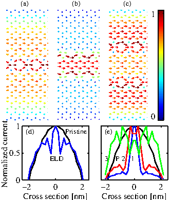
There is, however, another point worth mentioning. In
Fig. 3.21 the colormaps show the normalized current
spectrum at
![]() in the cross sections of the ELD-ZGNRs described in Fig. 3.20. Figure 3.21-a shows the current spectrum of the
ELD-ZGNR(10,10). The current is zero close to the edges of the ribbon
and peaks near the center. This is demonstrated more clearly in
Fig. 3.21-d, which shows the current along one atomic
chain perpendicular to this channel (blue line). The black line of
Fig. 3.21-d illustrates the current density on the cross
section of the pristine ZGNR channel for reference.
in the cross sections of the ELD-ZGNRs described in Fig. 3.20. Figure 3.21-a shows the current spectrum of the
ELD-ZGNR(10,10). The current is zero close to the edges of the ribbon
and peaks near the center. This is demonstrated more clearly in
Fig. 3.21-d, which shows the current along one atomic
chain perpendicular to this channel (blue line). The black line of
Fig. 3.21-d illustrates the current density on the cross
section of the pristine ZGNR channel for reference.
|
The current spectrum for the 2ELD-ZGNR(8,4,8) is shown in Fig. 3.21-b. The situation is now different since most of the current is confined within the two ELDs. This, however, is the case only when the distance between the ELDs is smaller than the widths of the upper/lower regions. In the case where the width of the middle region is similar to the widths of the upper/lower regions, the current is spread more uniformly in the channel as shown in Fig. 3.21-c for the 2ELD-ZGNR(7,6,7) channel. Figure 3.21-e shows again the current along one atomic chain in the cross section of these ribbons. The current spectrum is localized in the middle of the channel in the 2ELD-ZGNR(8,4,8) channel (red line) compared to the pristine channel (black line). In a 2ELD-ZGNR(9,2,9) channel with a narrower middle region the current spectrum is localized even closer around the center (blue line). A large portion of the current is in general flowing around the ELD regions. The design capability to localize the current spectrum in the middle of the channel away from the edges will prove advantageous in the presence of edge roughness since the current in this case will be less affected. On the other hand, in the case of the 2ELD-ZGNR(7,6,7) channel the current spectrum tends to concentrate more close to the edges (green line).