


Previous worst case characterization techniques involved the anding
of all independent parameters to determine the worst case values of an
objective function. The probability of the occurrence of the anding
conditions is very low. Imposing such pessimistic variation requirement
on the circuit design leads to overdesign and strict constraints on its
performance. Furthermore, such an approach ignores the inherent
correlation that exists between the main input variables. It is a well known
fact that the statistical variables of the P- and N-channel MOSFET's
in a CMOS technology are strongly correlated as these parameters
are determined by the same fabrication steps. In a similar manner to the
procedure described in the previous section, one can generate the predicted
 and
and  distributions based on the assumed statistical
variable distributions. As the target values for the key parameters are
usually known
distributions based on the assumed statistical
variable distributions. As the target values for the key parameters are
usually known , one can scale the previous
generation distributions assuming variance scales in proportion to mean
to estimate the expected key statistical parameter distributions.
, one can scale the previous
generation distributions assuming variance scales in proportion to mean
to estimate the expected key statistical parameter distributions.
The mean and standard deviation of the and
distributions can be calculated from the resulting joint probability
distribution function (jpdf). Any meaningful statement about the
and variation must be a statistical one and
requires a preassigned probability level  . As an illustration,
the predicted statistical distributions of a 0.5
. As an illustration,
the predicted statistical distributions of a 0.5 m CMOS technology
is plotted in Fig. 6.1 together with the
m CMOS technology
is plotted in Fig. 6.1 together with the  limit contour. This corresponds to a 99.7% confidence level that the
manufactured MOSFET currents will be within this contour.
One can apply this limit to calculate the characteristics values
of and corresponding to slow, typical,
and fast conditions. Specifically:
limit contour. This corresponds to a 99.7% confidence level that the
manufactured MOSFET currents will be within this contour.
One can apply this limit to calculate the characteristics values
of and corresponding to slow, typical,
and fast conditions. Specifically:
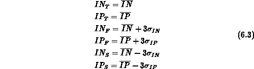
where  and
and  are the mean values,
  and
and  are the standard deviation determined from the simulated
distribution; The subscripts
are the standard deviation determined from the simulated
distribution; The subscripts  ,
,  , and
, and  denote the typical center
of the design area, and its high and low current corners respectively.
denote the typical center
of the design area, and its high and low current corners respectively.
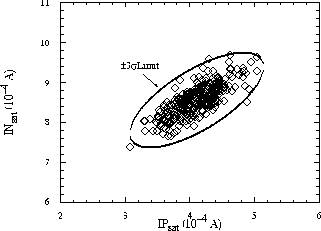
Figure 6.1:
Simulated and distributions for a  m CMOS
technology.
m CMOS
technology.
This statistical modeling capabilities provide the necessary framework for engineering parameter tolerances to specify the acceptable design space. By defining appropriate design objective criteria, other worst case conditions can also be defined. For example, the skewed corners corresponding to the mismatch conditions between the N-channel and P-channel currents can be determined by applying the same approach to generate the distribution of the current ratio:

which is calculated using the polynomial expressions in (6.2).
Again, the mismatch corner conditions can be calculated as the
limits of  :
:

Where  and
and  are the mean and standard deviation of ,
and the
are the mean and standard deviation of ,
and the  and
and  subscripts denote the fast N and slow P (FS), and slow
N fast P corners respectively.
subscripts denote the fast N and slow P (FS), and slow
N fast P corners respectively.