


Next: 2.5.2 Projection Printing
Up: 2.5 Optical System
Previous: 2.5 Optical System
A simple and straight forward approach is contact printing.
In contact printing, the mask
is pressed against the resist-coated wafer during exposure, i.e., the optical
part shown in Figure 2.3 or Figure 2.4 is
missing, but the other components like the illuminator and mask are kept.
An important
advantage is that feature sizes as small as 0.1  m can be
made using comparatively inexpensive equipment [18]. The mask
is held chrome-side down in intimate contact with the wafer.
Ideally, the gap between mask and wafer goes to zero, which minimizes diffraction
effects. The resolution is only limited by scattering effects that
might occur inside the resist due to its finite thickness.
In reality additional limitations of contact printing
result from the non-uniformity of mask and wafer.
This problem can be reduced by applying
pressures ranging from 0.05-0.3 atm. The major disadvantage of
such hard contact methods is the extremely high defect generation.
Defects are generated both on the wafer and mask during every contact
cycle. Mask lifetime is severely reduced and printed defect levels
are increased. Therefore, contact printing is only used in device research
or other applications that tolerate high defect rates.
m can be
made using comparatively inexpensive equipment [18]. The mask
is held chrome-side down in intimate contact with the wafer.
Ideally, the gap between mask and wafer goes to zero, which minimizes diffraction
effects. The resolution is only limited by scattering effects that
might occur inside the resist due to its finite thickness.
In reality additional limitations of contact printing
result from the non-uniformity of mask and wafer.
This problem can be reduced by applying
pressures ranging from 0.05-0.3 atm. The major disadvantage of
such hard contact methods is the extremely high defect generation.
Defects are generated both on the wafer and mask during every contact
cycle. Mask lifetime is severely reduced and printed defect levels
are increased. Therefore, contact printing is only used in device research
or other applications that tolerate high defect rates.
Proximity printing avoids defect generation because a small gap ranging from
10-50  m is introduced between mask and wafer. The separation
is usually controlled by a flow of nitrogen gas. The gas flow
keeps the mask away from the wafer surface. The main disadvantage of
proximity printing is a severe reduction in resolution due to diffraction
spreading. The achievable resolution is governed by the expression
m is introduced between mask and wafer. The separation
is usually controlled by a flow of nitrogen gas. The gas flow
keeps the mask away from the wafer surface. The main disadvantage of
proximity printing is a severe reduction in resolution due to diffraction
spreading. The achievable resolution is governed by the expression
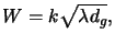 |
(2.5) |
whereby dg denotes the mask-to-wafer distance,
 is the exposure wavelength, and the
technology parameter k ranges between 1-2 depending on the
resist process. The square root behavior is a consequence of the Fresnel
diffraction theory valid in the near field
region just below the mask openings. For optical lithography,
typical values are k = 1.6,
is the exposure wavelength, and the
technology parameter k ranges between 1-2 depending on the
resist process. The square root behavior is a consequence of the Fresnel
diffraction theory valid in the near field
region just below the mask openings. For optical lithography,
typical values are k = 1.6,
 = 0.4
= 0.4  m, and
dg = 25
m, and
dg = 25  m,
yielding a resolution of W = 4
m,
yielding a resolution of W = 4  m. Resolution can be enhanced by
either decreasing the gap at the risk of contact and defect generation
or by reducing the wavelength. Using wavelengths
in the DUV or even EUV range will not suffice for optical proximity
printing to compete with projection printing. However, using X-rays
with a wavelength of about 1 nm feature sizes below
0.2
m. Resolution can be enhanced by
either decreasing the gap at the risk of contact and defect generation
or by reducing the wavelength. Using wavelengths
in the DUV or even EUV range will not suffice for optical proximity
printing to compete with projection printing. However, using X-rays
with a wavelength of about 1 nm feature sizes below
0.2  m
can be produced with proximity methods. This makes 1x proximity X-ray
a promising candidate for the 0.13
m
can be produced with proximity methods. This makes 1x proximity X-ray
a promising candidate for the 0.13  m and 0.10
  m
technology [3].
m
technology [3].
Next: 2.5.2 Projection Printing
Up: 2.5 Optical System
Previous: 2.5 Optical System
Heinrich Kirchauer, Institute for Microelectronics, TU Vienna
1998-04-17