


Next: 2.7.3 Electron-Beam
Up: 2.7 Nanolithography
Previous: 2.7.1 Extreme Ultraviolet
A promising technique already far evolved is 1x X-ray
proximity printing [26].
For soft X-rays with wavelengths ranging between
0.8-2 nm diffraction effects are negligible down to linewidths of
100 nm. The resolution is thus given by (2.5).
For example, an exposing wavelength of
 = 0.8 nm with a mask-to-wafer separation of
dg = 10
= 0.8 nm with a mask-to-wafer separation of
dg = 10  m and a process-related constant of k = 1.6
yields a resolution of 0.14
m and a process-related constant of k = 1.6
yields a resolution of 0.14  m. The variation in the
mask-to-wafer spacing reduces the achievable resolution and effectively
blurs the image. The following relationship can be derived
from (2.5),
m. The variation in the
mask-to-wafer spacing reduces the achievable resolution and effectively
blurs the image. The following relationship can be derived
from (2.5),
 |
(2.7) |
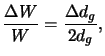
whereby the technology parameter k3 is kept constant. The tolerable
positioning error
 dg, i.e., the depth of focus thus equals the
maximally allowable linewidth change
dg, i.e., the depth of focus thus equals the
maximally allowable linewidth change
 W/W times twice the
distance dg. In the above example we have dg = 10
W/W times twice the
distance dg. In the above example we have dg = 10  m,
which yields a focal depth of 2
m,
which yields a focal depth of 2  m if 4% linewidth control is required.
This is a significant improvement upon optical projection printing
(cf. Figure 2.2).
Another big advantage of X-ray exposure is its negligible sensitivity
to small, low atomic
mass particles that frequently degrade image quality in optical lithography.
The great particle defect tolerance relieves clean room specifications
and increases process latitude. Severe problems arise from the fragility and
dimensional instability of the mask, and the high precision alignment
required due to the 1x replication method.
The starting material of the mask is usually a silicon wafer with a
borosilicate film on top. Subjecting the wafer to elevated temperatures
causes the boron to diffuse into the silicon. The resulting heavily-doped boron
film acts as an etch-stop, when the structure is etched from the backside to
form a thin silicon membrane.
The membrane is bonded to a pyrex support ring, and patterned with
a high atomic number material like gold to absorb the X-rays. The repair
of the costly X-ray masks is very important and can be accomplished by
photolytic or electron-beam induced deposition and ion beam sputter-erosion.
Another challenge is the development of bright X-ray sources for high volume
production. Two types of X-ray sources are available today, the synchrotron
and the laser-induced plasma radiation.
Due to the finite size of these sources they behave similarly to partially
coherent optical sources. The arising phenomenon is usually
called penumbral blurring since it has been considered to be problematic.
Recent work indicates that some penumbra has the beneficial effect
of washing out diffraction peaks at exposure boundaries caused by
coherency. Modern sources have sufficient intensity
to provide an optimum penumbral blur for a given design rule.
Finally, special resists have to be
developed further to minimize the effect of secondary electron processes. The
usage of low atomic number resist materials like carbon and oxygen reduces
the spreading of the exposure volume, because the energy of the
generated photoelectrons is then lower, which prevents them to travel far away
once they are released in the resist.
m if 4% linewidth control is required.
This is a significant improvement upon optical projection printing
(cf. Figure 2.2).
Another big advantage of X-ray exposure is its negligible sensitivity
to small, low atomic
mass particles that frequently degrade image quality in optical lithography.
The great particle defect tolerance relieves clean room specifications
and increases process latitude. Severe problems arise from the fragility and
dimensional instability of the mask, and the high precision alignment
required due to the 1x replication method.
The starting material of the mask is usually a silicon wafer with a
borosilicate film on top. Subjecting the wafer to elevated temperatures
causes the boron to diffuse into the silicon. The resulting heavily-doped boron
film acts as an etch-stop, when the structure is etched from the backside to
form a thin silicon membrane.
The membrane is bonded to a pyrex support ring, and patterned with
a high atomic number material like gold to absorb the X-rays. The repair
of the costly X-ray masks is very important and can be accomplished by
photolytic or electron-beam induced deposition and ion beam sputter-erosion.
Another challenge is the development of bright X-ray sources for high volume
production. Two types of X-ray sources are available today, the synchrotron
and the laser-induced plasma radiation.
Due to the finite size of these sources they behave similarly to partially
coherent optical sources. The arising phenomenon is usually
called penumbral blurring since it has been considered to be problematic.
Recent work indicates that some penumbra has the beneficial effect
of washing out diffraction peaks at exposure boundaries caused by
coherency. Modern sources have sufficient intensity
to provide an optimum penumbral blur for a given design rule.
Finally, special resists have to be
developed further to minimize the effect of secondary electron processes. The
usage of low atomic number resist materials like carbon and oxygen reduces
the spreading of the exposure volume, because the energy of the
generated photoelectrons is then lower, which prevents them to travel far away
once they are released in the resist.
Next: 2.7.3 Electron-Beam
Up: 2.7 Nanolithography
Previous: 2.7.1 Extreme Ultraviolet
Heinrich Kirchauer, Institute for Microelectronics, TU Vienna
1998-04-17