However, because of structural or chemical defects in organic semiconductors,
the motion of carriers is typically described by hopping transport, which is
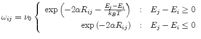
a phonon-assisted tunneling mechanism from site to site (Fig 1.2). Many
hopping models are based on the Miller-Abrahams equation [7]. In this model hopping from a
localized state ![]() to a state
to a state ![]() takes place at frequency
takes place at frequency ![]() ,
corrected for a tunneling probability and the probability to absorb a phonon
for hops upwards in energy:
,
corrected for a tunneling probability and the probability to absorb a phonon
for hops upwards in energy:
|
In organic solids, interactions are mainly covalent, but intermolecular interactions are due to much weaker van der Waals and London forces. These organic semiconductors typically have narrow energy bands, the highest occupied molecular orbital (HOMO) and the lowest unoccupied molecular orbital (LUMO), which can be easily disrupted by disorder. Thus, even in molecule crystals, the concepts of allowed energy band is of limited validity and excitations and interactions localized on individual molecules play a predominant role. The charge transport sites have a Gaussian distribution of energies and are localized [8]. The shape of the density of states (DOS) is suggested to be Gaussian based on the observed Gaussian shape of the optical spectra [9].
Transport energy [10] is a useful concept for the analysis of hopping transport in organic semiconductors. Importance of the transport energy stems from the fact that this is the energy that maximizes the probability for a carrier to hop upward in energy. It does not depended on the carrier initial energy, thus serving as an analog to the mobility edge.
For polycrystalline organic semiconductor layers, the temperature dependent transport data is often interpreted in terms of a multiple trapping and release model [11,12]. In this model the organic semiconductor film consists of crystallites which are separated from each other by amorphous grain boundaries. In the crystallites the carriers are delocalized, while the carriers in the grain boundaries become trapped in localized states. The transport description in terms of trapped carriers that can be thermally activated to transport level, is very similar to hopping transport as discussed above.
![\includegraphics[width=5.5cm]{figures/fem/band.eps}](img100.png)
![\includegraphics[width=6cm]{figures/fem/hop.eps}](img101.png)