Next: 7.3 Device Model for
Up: 7. Organic Semiconductor Device
Previous: 7.1 Introduction
Subsections
In this section we derive a basic expression for the sheet conductance based
on the variable range hopping (VRH) theory. This theory describes thermally activated tunneling
of carriers between localized states around
the Fermi level in the tail of a Gaussian distribution. It has been
used to calculate the mobility of OTFTs successfully. After some
simplification for the surface potential, simple and efficient
analytical expressions for the transfer characteristics and output
characteristics are obtained. The model does not require as input
parameters the explicit definition of the threshold and saturation voltage,
which are rather difficult to evaluate for this kind of device. The
obtained results are in good agreement with experimental data.
Because most organic films have an amorphous structure and disorder is dominating
the charge transport, variable-range-hopping in positionally and
energetically disordered systems of localized states is widely accepted as the
conductivity mechanism in organic semiconductors. Different from hopping,
where the charge transport is governed by the thermally activated tunneling
of carriers between localized states rather than by the activation of
carriers to the extended-state transport level, the concept of variable range
hopping means that a carrier may either hop over a small distance with high
activation energy or hop over a long distance with a low activation
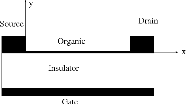
energy. In an organic thin film transistor with a typical structure shown in
Fig 7.1, an applied gate voltage gives rise to an accumulation of
carriers in the region of the organic semiconductors
Figure 7.1:
Schematic structure of an organic thin film transistor.
|
|
close to the insulator. As the carriers in the accumulation layer
fill the low-energy states of the organic semiconductor, any additional carrier
in the accumulation layer will require less activation energy to hop to
a neighboring site. This results in a higher mobility with increasing gate
voltage. In combination with percolation theory, Vissenberg studied the
influence of temperature and the influence of the filled states on the
conductivity based on the variable range hopping theory. The
expression for the conductivity as a function of the temperature and carrier
concentration is given by [43]
where  is a prefactor,
  is an effective overlap
parameter, which governs the tunneling process between two localized states,
and
is an effective overlap
parameter, which governs the tunneling process between two localized states,
and  2.8 is the critical number of bonds per site in the percolating
network [131],
2.8 is the critical number of bonds per site in the percolating
network [131],  is the effective temperature,
  is the number
of states per unit volume and
is the number
of states per unit volume and  is the fraction of the localized states
occupied by a carrier. The carrier concentration
is the fraction of the localized states
occupied by a carrier. The carrier concentration
 can be expressed in equilibrium as
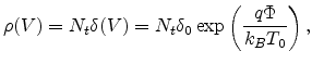 |
(7.1) |
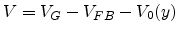
where  is the electrostatic potential,
and the
is the electrostatic potential,
and the  is the carrier occupation far from the organic-insulator
interface.
For an amorphous TFT the drain current
is the carrier occupation far from the organic-insulator
interface.
For an amorphous TFT the drain current  can be
expressed as
can be
expressed as
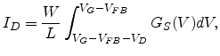 |
(7.2) |
where  is the channel width,
  is the channel length,
  is the
flat-band voltage, and
is the
flat-band voltage, and  is the sheet conductance of the channel at
 V. The potential
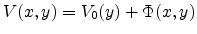
  is defined as
 , where
  is
the potential at the edge of the space-charge layer where there is no band
bending.
is
the potential at the edge of the space-charge layer where there is no band
bending.
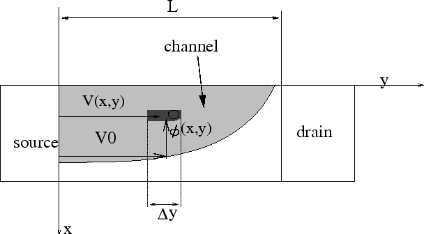
Figure 7.2:
Geometric definition.
|
|
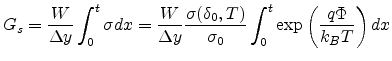
The basic definition of the channel configuration and the variables for the OTFT
investigated are illustrated in Fig 7.2.
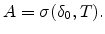
![$\displaystyle \sigma(\delta,T) = \sigma_0 \left[\frac{\pi N_t\delta(T_0/T)^3}{(2\alpha)^3B_c\Gamma(1-T/T_0)\Gamma(1+T/T_0)}\right]^{T_0/T},$](img576.png) |
(7.3) |
The electrostatic potential in the space charge layer at the point ( ) in the channel is expressed as
 , where the
  is the amount of the band bending in
the channel. The conductance for an element of channel length
is the amount of the band bending in
the channel. The conductance for an element of channel length  and the
width can be written as
and the
width can be written as
 |
(7.4) |
where  is the thickness of the organic layer.
Changing the variable of integration yields
is the thickness of the organic layer.
Changing the variable of integration yields
 |
(7.5) |
where  is the surface band bending and
 With
the identity
we obtain
In order to solve (7.5) we need to get an expression for
With
the identity
we obtain
In order to solve (7.5) we need to get an expression for  . By solving
Poisson's equation in the gradual channel approximation
. By solving
Poisson's equation in the gradual channel approximation
 |
(7.6) |
we obtain the electric field.
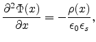
![$\displaystyle -F_x=\frac{\partial\Phi}{\partial x}\approx\sqrt{\frac{2k_BT_0N_t\delta_0}{\epsilon_0\epsilon_s}}.\exp\left[\frac{q\Phi(x)}{2k_bT_0}\right]$](img589.png) |
(7.7) |
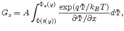
From (7.5) and (7.7) we obtain
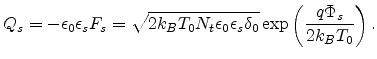
![$\displaystyle G_s=A\int_{\Phi(t)}^{\Phi_s}\exp\left[\frac{q\Phi}{k_B}\left(\frac{1}{T}-\frac{1}{2T_0}\right)\right]d\Phi.$](img590.png) |
(7.8) |
An expression for  is required. The surface charge density
  is related to by
 |
(7.9) |
The surface band bending is related to the applied gate voltage by
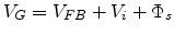 |
(7.10) |
where  is the voltage drop across the insulator,
 |
(7.11) |
where
 is the insulator capacitance per unit area.
From the equations above, an expression for is obtained
is the insulator capacitance per unit area.
From the equations above, an expression for is obtained
 |
(7.12) |
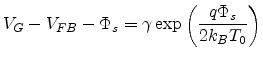
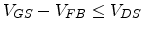
For an accumulation mode OTFT, the surface potential is negative,
 , corresponding to
  .
.
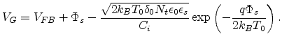 |
(7.13) |
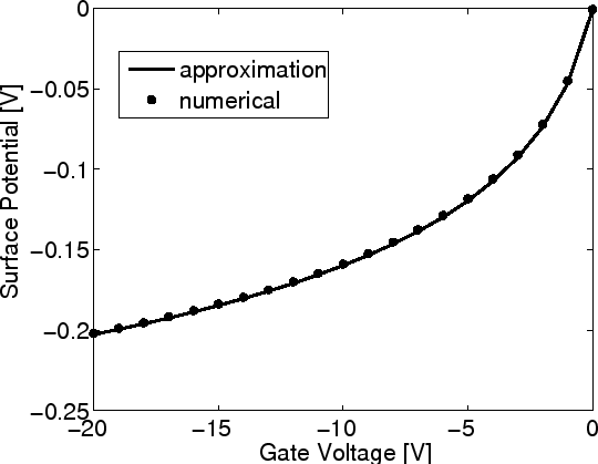
In order to reduce computation time, an explicit yet accurate relation between
surface potential and gate voltage is preferable. In (7.13) we can get using
a numerical approach. However, in the accumulation mode, it holds
 ,
so that an approximate expression of surface potential can be obtained as
,
so that an approximate expression of surface potential can be obtained as
![$\displaystyle \Phi_s=-\frac{2k_BT_0}{q}\ln\left[\frac{(V_{FB}-V_G)C_i}{\sqrt{2K_bT_0\delta_0N_t\epsilon_0\epsilon_s}}\right].$](img603.png) |
(7.14) |
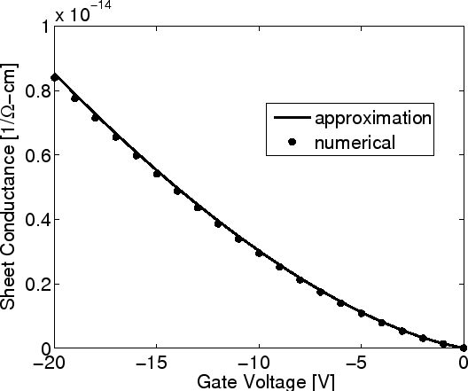
A comparison between numerical calculation and approximate calculation is
shown in Fig 7.3 and Fig 7.4. As can be seen, the agreement is very satisfactory.
Parameters are from [132,133].
With the simplified surface potential and (7.8) we can get the simplified
sheet conductance as
![$\displaystyle G_s=\beta\left[\left(\frac{V_G-V_{FB}}{\varrho}\right)^{2T_0/T-1}-1\right]$](img604.png) |
(7.15) |
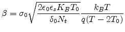
For a thick organic semiconductor layer,  and the coefficient
 is
is
Figure 7.3:
The electrostatic surface potential as a function of gate voltage obtained
by the implicit relation (7.13) and the approximation (7.14) (solid line).
|
|
Figure 7.4:
Sheet conductance from numerical calculation (symbols) and
the approximation.
|
|
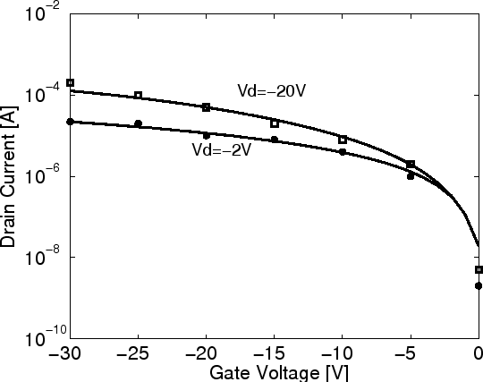
Figure 7.5:
Measured (symbols) and calculated transfer characteristics of a pentacence OTFT at
room temperature.
|
|
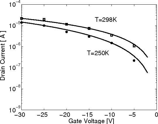
Figure 7.6:
Measured (symbols) and calculated transfer characteristics of a pentacence OTFT at
different temperatures at  .
.
|
|
The drain current can be calculated by substituting the expression for  into (7.2). We obtain
![$\displaystyle I_D=\beta\frac{W}{L}\left[{\left(\frac{V_G-V_{FB}}{\varrho}\right)^{2T_0/T}-\left(\frac{V_G-V_{FB}-V_D}{\varrho}\right)^{2T_0/T}}\right]$](img612.png) |
(7.16) |
in the triode region (
 ) and
) and
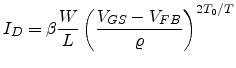 |
(7.17) |
in saturation (
 ).
).
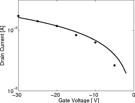
Figure 7.7:
Measured (symbols) and calculated transfer characteristics of a PTV OTFT at
room temperature at .
|
|
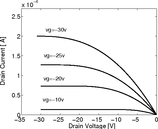
Figure 7.8:
Modeled output characteristics of a pentacene OTFT.
|
|
This model has been confirmed by comparisons between experimental data and
simulation results. Input parameters are taken from [132]:
 ,
,
 ,
,
 ,
,
 ,
,
 ,
,
 ,
,  .
.
In Fig 7.5 and Fig 7.6 the transfer characteristics of a
pentacene OTFT are given for  at different drain voltage and different temperature.
Both figures show a good agreement between the analytical model and
experimental data. Here we also model the transfer characteristics of a PTV
OTFT, where some parameters are different from those for pentacence:
at different drain voltage and different temperature.
Both figures show a good agreement between the analytical model and
experimental data. Here we also model the transfer characteristics of a PTV
OTFT, where some parameters are different from those for pentacence:
 K,
K,
 S/m,
S/m,
 , as shown in Fig 7.7. The
modeled output characteristics of the pentacene OTFT is shown in Fig
7.8.
, as shown in Fig 7.7. The
modeled output characteristics of the pentacene OTFT is shown in Fig
7.8.
Next: 7.3 Device Model for
Up: 7. Organic Semiconductor Device
Previous: 7.1 Introduction
Ling Li: Charge Transport in Organic Semiconductor Materials and Devices
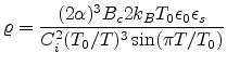
![$\displaystyle A=\sigma_0\left[\frac{N_t\delta_0(T_0/T)^4\sin(\pi T/T_0)}{B_c(2\alpha)^3}\right]^{T_0/T}
$](img586.png)