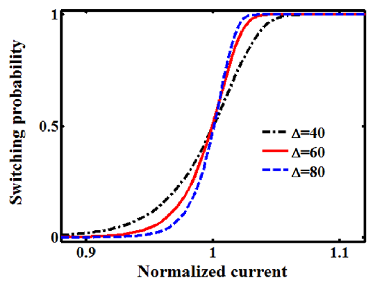
| Figure 4.23.: | Switching dynamics of the MTJ device as function of the applied current plotted for different values of  . .
|
| Figure 4.23.: | Switching dynamics of the MTJ device as function of the applied current plotted for different values of .
|
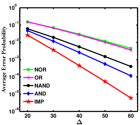
| Figure 4.24.: | Average error probabilities for the basic operations of the two-input reprogrammable gate (AND, OR,
NAND, and NOR) and the proposed CC-IMP gate (IMP) as a function of  for for  . . |
As mentioned before, the TMR ratio is considered as a very important device parameter for the reliability of
the conditional switching in MTJ-based logic gates. However, other MTJ device parameters also affect the
reliability. Fig. 4.23 shows the switching probabilities of the MTJ device in the thermally-activated switching
regime (Eq. 4.15) as a function the MTJ current for different values of the thermal stability factor  . It
illustrates that a higher
. It
illustrates that a higher  provides sharper switching dynamics (switching windows shown in Fig. 4.19 and
Fig. 4.13). As decreasing the SWs increases the width of the reliable gaps opened between the SWs of the
desired and undesired switching events, we expect a more reliable logic behavior for a higher
provides sharper switching dynamics (switching windows shown in Fig. 4.19 and
Fig. 4.13). As decreasing the SWs increases the width of the reliable gaps opened between the SWs of the
desired and undesired switching events, we expect a more reliable logic behavior for a higher  .
In fact, according to Eq. 4.15, the dominant term for the switching probability calculation is
.
In fact, according to Eq. 4.15, the dominant term for the switching probability calculation is
![exp [- Δ (1 - I ∕I )]
C0](diss1021x.png) . The modulation of the term
. The modulation of the term  depends on the TMR ratio and its
impact has been studied before. Nevertheless, a higher
depends on the TMR ratio and its
impact has been studied before. Nevertheless, a higher  magnifies the effect of this modulation.
Therefore, for all MTJ-based logic operations, a higher
magnifies the effect of this modulation.
Therefore, for all MTJ-based logic operations, a higher  decreases the error probabilities.
Indeed, Fig. 4.24 shows the average error probabilities of the basic operations of the CC-IMP
and the two-input reprogrammable gates as a function of the thermal stability factor
decreases the error probabilities.
Indeed, Fig. 4.24 shows the average error probabilities of the basic operations of the CC-IMP
and the two-input reprogrammable gates as a function of the thermal stability factor  . It
illustrates that the error decreases exponentially with
. It
illustrates that the error decreases exponentially with  and for the same device characteristics and
 , the CC-IMP gate exhibits always a more reliable logic behavior as compared to the
two-input reprogrammable gate. At each point the circuit parameters (
, the CC-IMP gate exhibits always a more reliable logic behavior as compared to the
two-input reprogrammable gate. At each point the circuit parameters ( and
and  in Fig. 4.15b
and
in Fig. 4.15b
and  in Fig. 4.20) are optimized to minimize the error probability. As it is shown in [38],
although a lower
in Fig. 4.20) are optimized to minimize the error probability. As it is shown in [38],
although a lower  value allows easier STT switching, a minimum value of
 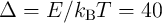 is
required for low write and read error rates in STT-MRAM technology. A similar trade-off is
encountered in the design of the MTJ-based logic gates. According to Eq. 4.15, the error values are
independent of the absolute values of
is
required for low write and read error rates in STT-MRAM technology. A similar trade-off is
encountered in the design of the MTJ-based logic gates. According to Eq. 4.15, the error values are
independent of the absolute values of  and
and  , as the computations can be generalized by
normalizing all current and resistance values to
, as the computations can be generalized by
normalizing all current and resistance values to  and
and  , respectively. Furthermore, the
effect of the pulse durations (
, respectively. Furthermore, the
effect of the pulse durations ( ) is negligible as compared to the internal exponential term in
Eq. 4.15.
) is negligible as compared to the internal exponential term in
Eq. 4.15.
In order to investigate the effect of the MTJ device-to-device variations, Fig. 4.25 shows the expectation
value for the NIMP error probabilities ( ) as a function of
  under MTJ device variations with
Gaussian distribution [191]. The spread of the variations (
under MTJ device variations with
Gaussian distribution [191]. The spread of the variations ( ) is assumed to be 4% in
  , TMR
ratio and
, TMR
ratio and  [191] for both target and source MTJs (
 ). The mean values (
 ) for TMR ratio and
  are equal to 250% and
  , respectively. For each point, circuit parameters are fixed to the values
which minimize the error and the average error probability for all combinations of input states (
, respectively. For each point, circuit parameters are fixed to the values
which minimize the error and the average error probability for all combinations of input states ( )
with 10000 random variations is calculated. Then the expectation error values are obtained by
)
with 10000 random variations is calculated. Then the expectation error values are obtained by
 , where
  is the distribution function of the errors (shown inset in
Fig. 4.25). As it is expected, MTJ device variations increase the error probabilities as shown in
Fig. 4.25.
is the distribution function of the errors (shown inset in
Fig. 4.25). As it is expected, MTJ device variations increase the error probabilities as shown in
Fig. 4.25.
 ) as a function of
  .
.