5.3 Implementation of the Improved Implication Architecture
5.3.1 Structural Asymmetry
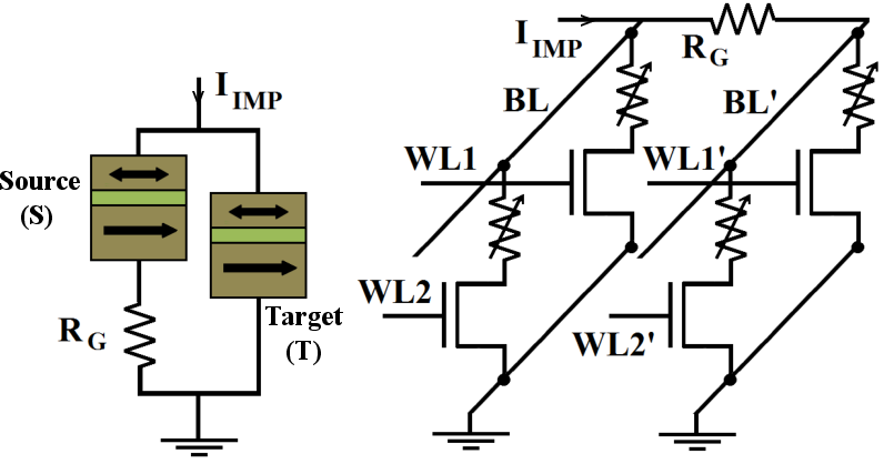
By replacing the MTJ devices with 1T/1MTJ cells, the implication logic gates are realized in MRAM arrays
to provide large-scale non-volatile magnetic circuits (Fig. 5.3). Due to the structural asymmetry caused by
 , two MRAM arrays are required in this asymmetric implementation. For performing the implication
operation, a source (target) MTJ can be selected only in the source (target) MRAM array which is (not)
serially connected to
, two MRAM arrays are required in this asymmetric implementation. For performing the implication
operation, a source (target) MTJ can be selected only in the source (target) MRAM array which is (not)
serially connected to  . Although this architecture enables independent STT writing of the input MTJs to
eliminate the difference between reading, writing, and performing logic operations, intermediate read/write
operations are required to readout the output of any logic operation from the target array and
to write it in the source array as an input for the next logic steps. In fact, as there is a need
for a physical resistor
. Although this architecture enables independent STT writing of the input MTJs to
eliminate the difference between reading, writing, and performing logic operations, intermediate read/write
operations are required to readout the output of any logic operation from the target array and
to write it in the source array as an input for the next logic steps. In fact, as there is a need
for a physical resistor  which is connected in series to
  ,
,  (
( ) can be used only as
source (target) MTJ for the implication operations and the logic result stored in
) can be used only as
source (target) MTJ for the implication operations and the logic result stored in  cannot be
used as a source input for the next implication operation. Therefore, performing implication
operation between two inputs from the same array is not possible without intermediate read/write
operations.
cannot be
used as a source input for the next implication operation. Therefore, performing implication
operation between two inputs from the same array is not possible without intermediate read/write
operations.
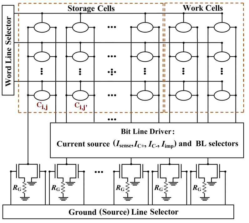
Fig. 5.4 shows a simplified implication logic circuit architecture based on the STT-MRAM architecture to
realize the MTJ-based current-controlled implication gate (Fig. 5.4). This circuit enables stateful logic for
which the need of using extra charge-based logic gates is eliminated and the memory cells serve
simultaneously as logic gates and latches via implication operation. The implication operation between two
cells C and C
and C (
( ) can be performed by simultaneous selection of the
  -th WL, the
 -th (target) and the
  -th (source) SLs which are connected to the ground directly and via
  ,
respectively, and by applying the current source
,
respectively, and by applying the current source  to the
  -th and
  -th BLs. The result of the
implication operation is written in C
-th BLs. The result of the
implication operation is written in C .
.
Compared to the common STT-MRAM architecture, the SL and the BL drivers are more complicated as they
have to provide more selection capabilities. Furthermore, two work cells are added to each WL,
since it has been shown that with two additional memory elements all Boolean functions can be
performed on any number of the storage cells [194]. These work cells can also be used to connect
different WLs. Indeed, in order to perform the implication between memory cells from different
WLs, one has to copy the logic data stored in a memory cell into a work cell from the other
WL. This increases the required time and energy consumption and limits the flexibility of the
computation.
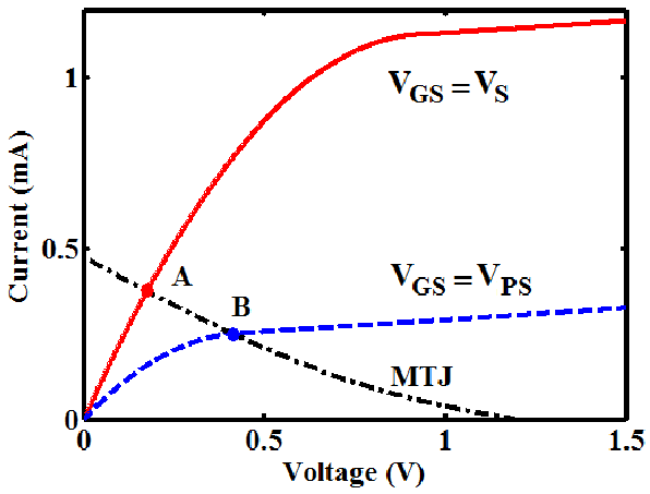
It should be noted that the nonzero ON resistance of the access transistors ( ) decreases the effective
TMR ratio of the 1T/1MTJ cells which can be defined as
) decreases the effective
TMR ratio of the 1T/1MTJ cells which can be defined as
 | (5.5) |
Therefore, a robust implication operation needs MTJs with sufficiently high TMR ratio and electrical
resistance. According to Fig. 4.17b, an implication reliability of 99.9% requires a TMR ratio higher than
250% when the effective TMR ratio of a 1T/1MTJ is decreased by about 10%-30% based on the MTJ and
the transistor devices characterized in [49].
5.3.2 Addressing the Asymmetry Issue
The inherent asymmetry of the proposed implication logic gate causes a significant limitation in the flexibility
of the computations and forces extra read/write operations in the MRAM-based architectures shown in
Fig. 5.3 and Fig. 5.4 as discussed before. This problems can be addressed by an innovative
solution for the asymmetry issue by using the access transistors as voltage-controlled resistors to
eliminate the need for a physical  . If voltage pulses with different amplitudes are applied to the
different WLs, the transistors have different bias points (Fig. 5.5) and thus exhibit different channel
resistances. Fig. 5.6a shows the MTJ- and the MRAM-based CC-IMP circuit topologies. In the
MRAM array, the structural asymmetry required for the CC-IMP is provided, when the select and
pre-select voltage signals (
. If voltage pulses with different amplitudes are applied to the
different WLs, the transistors have different bias points (Fig. 5.5) and thus exhibit different channel
resistances. Fig. 5.6a shows the MTJ- and the MRAM-based CC-IMP circuit topologies. In the
MRAM array, the structural asymmetry required for the CC-IMP is provided, when the select and
pre-select voltage signals ( and
and  ) are applied to two arbitrary WLs. As
  , the
transistors exhibit different channel resistances and the required structural asymmetry is implicitly
provided by the pre-selected transistor featuring a higher resistance which acts as
, the
transistors exhibit different channel resistances and the required structural asymmetry is implicitly
provided by the pre-selected transistor featuring a higher resistance which acts as  . The logic
operation is performed by applying simultaneously the current
. The logic
operation is performed by applying simultaneously the current  to the common BL and
  and
and
 to the WLs of the target and the source 1T/1MTJ cells, respectively. The logic result is
stored as the final resistance state of the selected (target) MTJ, which can be used now as a
source input by pre-selection in the next operations. This significantly reduces the complexity,
energy consumption, and delay as it eliminates the need for extra hardware like the source line
selector shown required in the MRAM architecture (shown Fig. 5.4) as well as the intermediate
read/write operations needed for reading (writing) the target (source) data of the current (next) logic
stage.
to the WLs of the target and the source 1T/1MTJ cells, respectively. The logic result is
stored as the final resistance state of the selected (target) MTJ, which can be used now as a
source input by pre-selection in the next operations. This significantly reduces the complexity,
energy consumption, and delay as it eliminates the need for extra hardware like the source line
selector shown required in the MRAM architecture (shown Fig. 5.4) as well as the intermediate
read/write operations needed for reading (writing) the target (source) data of the current (next) logic
stage.
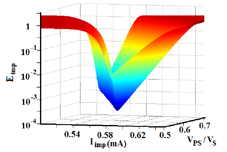
Fig. 5.6b shows the required circuit signals to implement the universal NOR operation ( )
in three steps, one TRUE and two NIMP operations, as shown in Eq. 3.2. According to Eq. 4.27, the
reliability of the implication-based NOR is then obtained as
)
in three steps, one TRUE and two NIMP operations, as shown in Eq. 3.2. According to Eq. 4.27, the
reliability of the implication-based NOR is then obtained as  which is
 for
for  . For a given MTJ and transistor device characteristics, the values of the
circuit parameter (
. For a given MTJ and transistor device characteristics, the values of the
circuit parameter ( and
and  ) are optimized (Fig. 5.7) by using Eq. 5.1 and the reliability model
presented in the previous chapter.
) are optimized (Fig. 5.7) by using Eq. 5.1 and the reliability model
presented in the previous chapter.
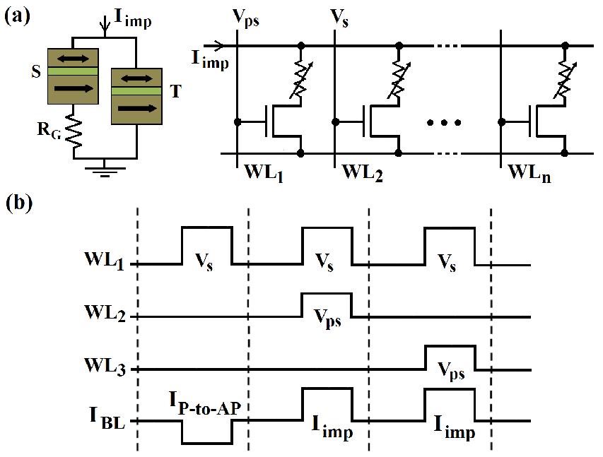
 . (b) Circuit
signals for performing the universal NOR operation in MRAM-based implication logic architecture.
. (b) Circuit
signals for performing the universal NOR operation in MRAM-based implication logic architecture.