Figure 7.1: Schematic illustration of penta-layer MTJs.
First, the influence of the reference layers on switching time of the penta-layer nanopillar structure (Figure 7.1) is investigated. The model geometry of the nanopillar is defined as CoFe(8nm)/AlOx(0.7nm)/Py(4nm)/Cu(6nm)/CoFe(5nm) (Py is Ni81Fe19), with an elliptical cross-section with 90- and 35-nm axes [66]. In the structure the different spacer layers are used to keep the difference in the magnetoresistance between the two states. This leads to an asymmetric switching time due to the different torques associated with the different spacer layers and therefore the structures require optimization.
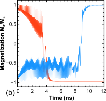
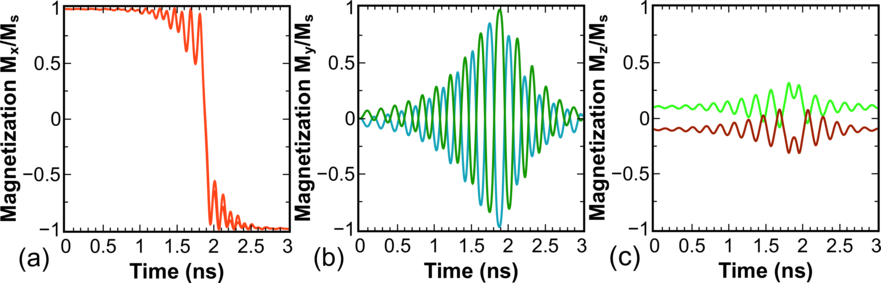
The employed parameters for the simulations are shown in Table 7.1. Figure 7.2a demonstrates an evolution of the average magnetization in the free magnetic layer during switching. A compensating external magnetic field is introduced. The results are in good agreement with those for the same elliptical cross-section at 77K reported in [64]. The difference between the switching times from parallel to anti-parallel (with respect to the oxide tunnel junction) configuration increases when the compensating magnetic field is turned off (Figure 7.2b). The compensation can also be achieved by modifying the thicknesses of the fixed ferromagnetic layers and/or the distances between the layers. This opens the way for an optimization of the penta-layers structure.
| Symbol | T=77K | T=300K |
| η1 | 0.3 | 0.3 |
| η2 | 0.35 | 0.35 |
| γ | 2.3245⋅105 m/(A⋅s) | 2.3245⋅105 m/(A⋅s) |
| α | 0.01 | 0.01 |
| A | 1.3⋅10-11 J/m | 1.1⋅10-11 J/m |
| MS | 644⋅103 A/m | 560⋅103 A/m |
| MSp | 1.15⋅106 A/m | 1⋅106 A/m |
| η1 - for MTJ with dielectrical spacer
| ||
| η2 - for GMR with metal spacer
| ||
| MSp1 = MSp2 = MSp
| ||
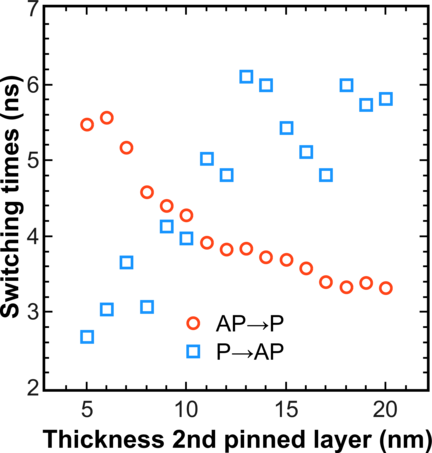
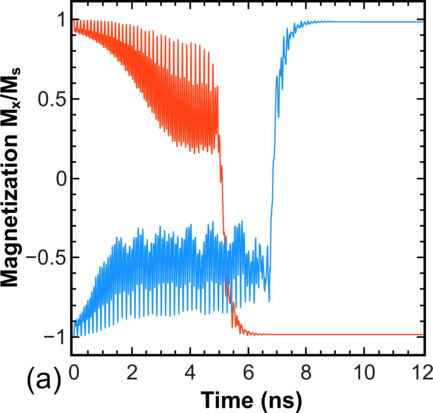
In the following, the influence of the thicknesses of the fixed layers on the in-plane magnetostatic field in the free magnetic layer is investigated. The corresponding dependence is shown in Figure 7.3. Each point is the result of statistical averaging with respect to 15 different realizations of the switching process. It demonstrates that the switching time from parallel to anti-parallel configuration and vice versa depends strongly on the fixed layer thickness. The most symmetric switching is achieved when the second fixed layer thickness is around 9-10 nm.
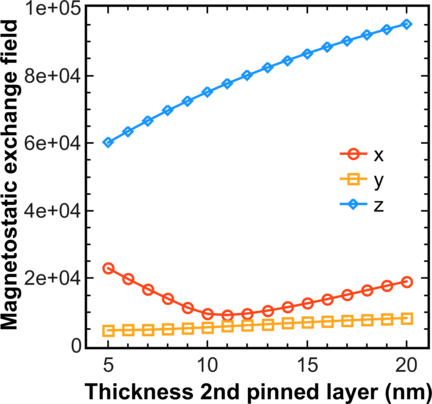
It is interesting to note that the switching time is shorter, when the compensation is achieved by modifying the thicknesses of the fixed ferromagnetic layers than in the case of an applied external field. To find the reason for this discrepancy, one should have in mind that by varying the thickness of the fixed layer, one can only compensate the in-plane component of the magnetostatic field. At the same time, the field projection perpendicular to the plane is not compensated. The absolute value of the average field orthogonal to the plane of the free layer is shown in Figure 7.4. This field component facilitates switching and explains the reduction in switching time.
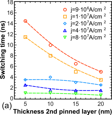
In order to make the system thermally stable at room temperature, the thickness of the free layer is increased from 4nm to 4.5nm, and the elliptical cross-section axes to 120 and 40 nm, correspondingly. Figure 7.5 displays the dependences of the switching times as a function of the fixed layer thickness at different current densities. As the current increases, the switching time decreases, as expected. Interestingly, the dependence of the switching time on the thickness vanishes at large current densities. This signifies that the magnetostatic coupling between the fixed and the free layers becomes irrelevant at high current densities. It is to note again that, at low current densities, an optimization of a particular penta-layer structure is required to achieve fast and symmetric switching behavior.
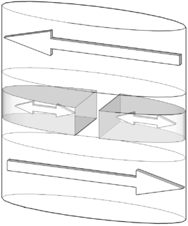
For a future optimization of the nanopillar the structure with a composite free layer is proposed. The structure with a composite ferromagnetic free layer is obtained by removing a central stripe of width s from the monolithic free layer (Figure 7.6). In a first step the structure CoFe/spacer oxide(1nm)/Py(4nm)/spacer oxide(1nm)/CoFe (Py is Ni81Fe19) with an elliptical cross-section (major axes 90nm and 35nm, and s =5nm, correspondingly) is investigated. In order to simplify the identification of the important features related to switching for such structures, it is assumed to be symmetric (the spacer layers are equivalent). It should be noted that for an asymmetric structure it is possible to apply the method described above to achieve a symmetric switching time.
Contrary to the standard consideration, it is not assumed the reference layers being fully compensated. They produce the magnetostatic field Hms, which couples the pinned layers and the free layer, thus offering an additional degree of freedom to improve the characteristics of the system.
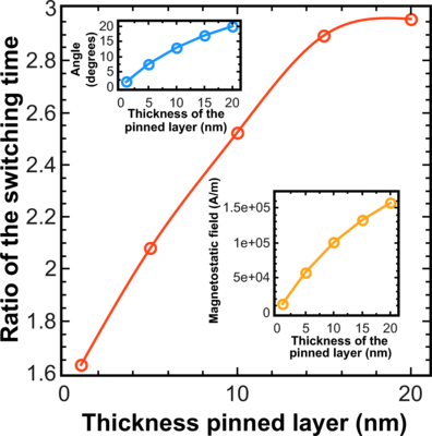
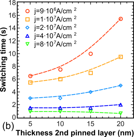
This non-compensated field causes the magnetization of the free layer to tilt out of the x - y plane. The non-zero angle between the fixed magnetization and the magnetization in the free layer results in an enhanced spin transfer torque, when the current starts flowing perpendicular to the x - y plane. In the case of the monolithic structure, however, the torque remains marginal in the central region, where the magnetization is along the x axis. As the amplitude of the end domains precession increases, the central region experiences almost no spin torque and preserves its initial orientation along the x axis, thus preventing the whole layer from alternating its magnetization orientation. This is, however, not the case when the central region is removed in the composite structure and the end domains become virtually independent. Figure 7.7 demonstrates a substantial decrease of the switching time in the penta-layer structure with the composite free layer, for the same current density, as a function of the thickness of the pinned ferromagnetic layers. The switching process for the pinned layer thicknesses of 5nm, 15nm, and 20nm is shown in Figure 7.8. Due to the removal of the central region, which represented the “bottleneck” for switching in the monolithic structure, the shape anisotropy energy decreases (Figure 7.8, inset). However, its value is still sufficiently large for guaranteeing the thermal stability at operation conditions [66].

The switching time in a penta-layer structure with a composite free layer is decreasing, if the thickness of the pinned layers is increased. This is due to the fact that the z-component of the magnetostatic field Hms (Figure 7.7, bottom inset) increases together with the pinned layer thickness, causing a larger initial angle (Figure 7.7, top inset) between the relaxed magnetization in the domains of the free layer and the magnetization of the pinned layer, a larger torque and, as a consequence, a shorter switching time.
In the section only a first description and raw explanation of the fast switching phenomena in the structure with the composite free layer was given. In the following the structure and phenomenon is discussed in detail.
For a more detailed study of the structure with composite free layer, CoFeB was considered as material for the free and reference layers (Table 7.2).
| Symbol | T=300K |
| η | 0.63 |
| γ | 2.3245⋅105 m/(A⋅s) |
| α | 0.005 |
| A | 1⋅10-11 J/m |
| K1 | 2⋅103 J/m3 |
| MS | 8.9⋅105 A/m |
| MSp1 = MSp2 = MSp = MS
| |

The dependence of the switching time on the aspect ratio of the free layer is investigated now. The aspect ratio is chosen so that for a composite free layer ((length - separation)∕2)∕width = 1.25. Figure 7.9 shows a decrease of the switching time in MTJs with a composite free layer as compared to that in MTJs with a monolithic free layer of similar dimensions, for all cross-section areas. Each point is a result of statistical averaging with respect to 50 different realizations of the switching process. The results clearly show a linear dependence of the switching time in the composite structures on the ratio area∕separation.
As discussed in Chapter 4 the critical parameter for the STT-MRAM is thermal stability, so the detailed investigation of the composite structure has to begin with the determination of this parameter. To find the switching path due to thermal agitations it is necessary to determine the state for which the barrier separating the two stable magnetization states in the free layer is minimal. Figure 7.10 shows that the switching path due to thermal agitations must go through the state with magnetizations of the halves opposite to each other (the C state in Figure 7.10).

Thus, the thermal stability factor for a composite structure is determined by the energy difference between the system in the state C (Figure 7.10) and the system with magnetization directed along the long axis of the ellipse.
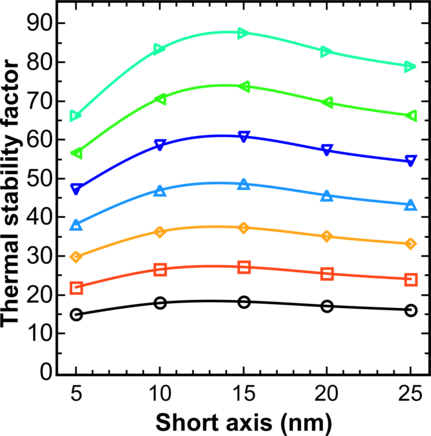
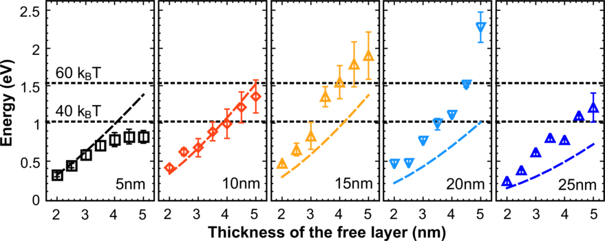
After determining the method of calculating the thermal stability factor for the composite structure, the influence of scaling the dimensions on the thermal stability factor for MTJs with a composite free layer must be investigated. Due to the removal of the central region from the monolithic structure, the shape anisotropy is slightly decreased together with the thermal stability factor. To boost the thermal stability factor, it is sufficient to increase the thickness of the free layer and/or the aspect ratio. Figure 7.11 shows the thermal stability factors of MTJs with a composite free layer as a function of the free layer thickness d. An MTJ with 52.5 × 10nm2 cross-section and d = 5nm free layer thickness has a thermal stability factor ~60kBT, which exceeds all of the single p-MTJs demonstrated to date [199].
The similarity of change of the thermal stability factor for the monolithic and composite free layer allows us to derive an analytical equation for the calculation of the thermal stability factor of the composite structure based on the analytical equation for the monolithic free layer. For monolithic free layer with elliptical cross-section (l > w ≫ d) the approximate value of the thermal stability factor is determined as [60]:
 | (7.1) |
Here, w and l are the dimensions of the ellipse along the short and long axis, respectively, and V m is the volume of the monolithic free layer. Similar to Equation 7.1, the approximate value of the thermal stability factor for composite free layer is described as:
 | (7.2) |
Here, a is a fitting parameter, V c = V m -w ⋅s⋅d is the volume of the composite free layer, where s is a distance between two parts of the composite free layer.
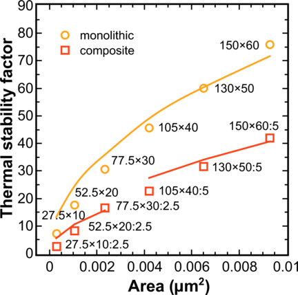
Figure 7.12 shows the result of the thermal stability factor simulations based on two different approaches. The fitting parameter a for the composite structure strongly depends on the separation and is equal to 2/3 for small separations (s = 2.5nm), and 3/4 for larger separations (s = 5nm).
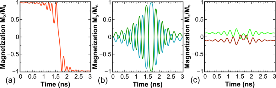
To reveal the reason for fast switching one has to look at the magnetization dynamics of the left and right part of the composite structure structure separately (Figure 7.13). A structure with an elliptical 52.5 × 25nm2 cross-section and the following layer sequence is considered: CoFeB(5nm)/MgO(1nm)/CoFeB(2nm)/MgO(1nm)/CoFeB(5nm). The central 2.5 nm stripe is removed from the middle CoFeB layer. Figures 7.13b and 7.13c show that the switching processes of the left and right parts of the composite free layer occur in opposite senses to each other. Most importantly, the magnetizations of each piece stay practically in-plane. Because the magnetization does not go out-of-plane, as during switching of the monolithic free layer, this switching behavior should lead to a decrease of the switching energy barrier. It turns out that the switching paths by current and due to thermal fluctuations are similar. Thus, as in p-MTJs, the switching barrier in the composite structure becomes practically equal to the thermal stability barrier defined by the shape anisotropy of the composite free layer structure. The reduction of the switching barrier leads to the reduction of the switching time in a composite structure as compared to a conventional MTJ at the same switching current density.
In the following the height of the thermal energy barrier is compared with that of the switching energy barrier (Figure 7.14). As expected from the analysis of the magnetization dynamics, the switching barrier becomes practically equal to the thermal stability barrier.
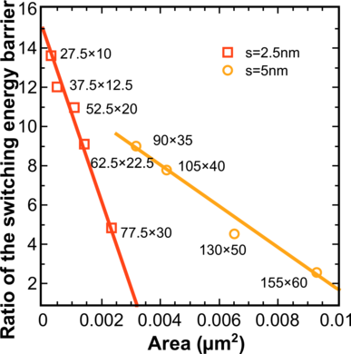
Figure 7.15 shows the ratio of the switching energy barrier in monolithic and composite structures. It displays an almost 14-fold decrease of the switching energy in MTJs with composite layer.
The equality of the switching and the thermal barriers in composite structures results in an almost linear increase of the switching time in these MTJs with increasing thickness of the free layer and/or aspect ratio, see Figure 7.16a. The dependence for the monolithic structure is shown in Figure 7.16b.
The influence of the MTJ geometry on the switching acceleration in MTJs with a composite free layer relative to the one with a monolithic layer is illustrated in Figure 7.17. The long axis is fixed at 52.5nm. Each point is a result of statistical averaging over 30 different realizations of the switching process. To decrease the switching time in the composite structure it is necessary to increase the thickness of the pinned layers. An almost threefold reduction of the switching time is achieved in MTJs with a composite free layer without compromising the thermal stability.
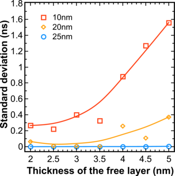
Now the standard deviations of the switching time distributions are compared in the monolithic and composite structure shown in Figure 7.18a. The width of the switching time distribution for MTJs with a composite free layer can be almost ~2000 times narrower than that for MTJs with a monolithic free layer. The dependence of the value of the standard deviation on composite layer thickness and aspect ratio is also shown in Figure 7.18b. An MTJ with 52.5 × 25nm2 cross-section has a standard deviation of the switching time ~ 10-3ns, while an MTJ with 52.5 × 10nm2 cross-section has the standard deviation of the switching time 0.3-1.6ns.
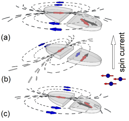
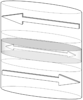
In order to find a physical explanation for the distribution narrowing, the switching process is analyzed in detail. A schematic illustration of the self-stabilization and self-acceleration principle of switching in a composite free layer is explained in Figure 7.19. Each half of the free layer generates a stray magnetic field which influences the other half and helps stabilizing the switching process. This stray magnetic field increases with growing short axis which leads to the switching times distribution narrowing. Before the moment when the magnetizations of the different halves of the composite layer are in opposite directions to each other (Figure 7.19b) the stray magnetic field acts as a stabilizing factor of switching (Figure 7.19a). After the opposite magnetization state the stray magnetic fields accelerate switching as illustrated in Figure 7.19c.
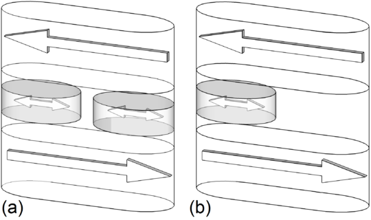
In this section a structural optimization of the composite free layer (see subsection 7.2) is presented by means of extensive micromagnetic simulations and a new structure for the composite free layer is proposed. To distinguish the two types of composite free layers, the notation for an MTJ with the free layer consisting of two equivalent parts of half-elliptic form separated by a narrow non-magnetic spacer is introduced as C-MTJ (Figure 7.6) and C2-MTJ for the new structure.
The free layer of the C2-MTJ (Figure 7.20a) is composed of two ellipses with the axes a∕2 and b inscribed into a rectangle a × b. Thus, the newly proposed structure does not require a narrow gap between the two parts of the composite layer, and therefore can be easily fabricated. Next, the most important parameters of STT-MRAM devices, switching time, thermal stability, and switching energy barrier of C2-MTJ, C-MTJ, conventional MTJ with monolithic free layer (Figure 7.1), and an M2-MTJ structure with one small free layer elliptical shape (Figure 7.20b) are compared.
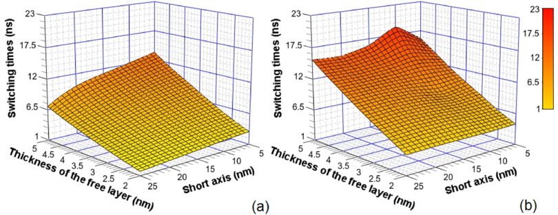
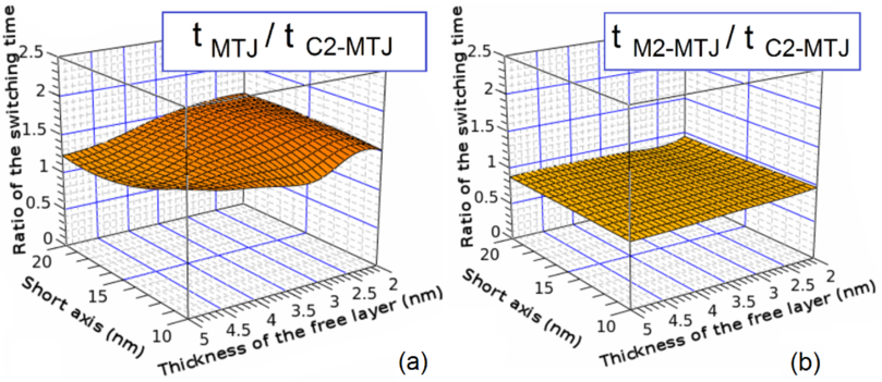
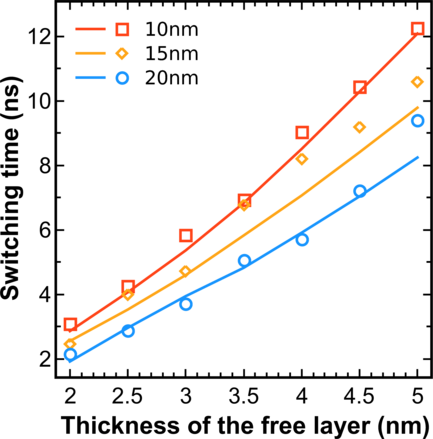
First, the switching times of C2-MTJs are discussed and compared with those of C-MTJs. Figure 7.21 shows the dependence of the switching time on the thicknesses of the free layer for three values of the short axis: 10nm, 15nm, and 20nm. The long axis is fixed at 52.5nm. The simulations demonstrate that C2-MTJs and C-MTJs have practically equal switching times for all considered cross-sections of the free layer.
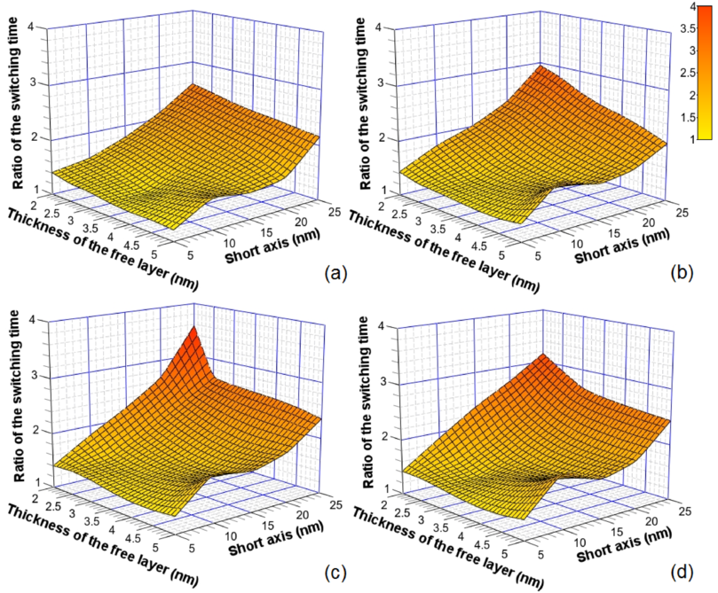
The fact that the switching times in C-MTJs and C2-MTJs are equal also means a switching acceleration for C2-MTJs as compared to the conventional MTJ with a monolithic free layer. This is indeed confirmed by the results of the simulations shown in Figure 7.22a. Figure 7.22b demonstrates that C2-MTJs display almost the same switching times as the structure with a single small ellipse (M2-MTJ, Figure 7.20b).
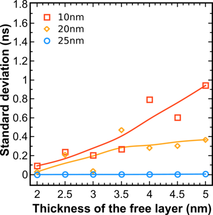
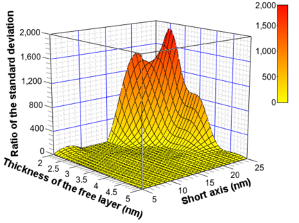
Now the standard deviations of the switching time distributions in C-MTJs and C2-MTJs are compared. The dependence of the value of the standard deviation on composite layer thickness and aspect ratio for C2-MTJ is shown in Figure 7.23. With 52.5 × 25nm2 cross-section a standard deviation of the switching time ~ 10-3ns is obtained for both structure, while with 52.5 × 10nm2 cross-section the standard deviation of the switching time is 0.3-1.6ns for the C-MTJ (Figure 7.18b) and 0.09-0.9ns for the C2-MTJ (Figure 7.23). Thus the C2-MTJ structure shows a ~2-3 times narrower distribution of the switching times as compared to the C-MTJ structure at large aspect ratio of the free layer.
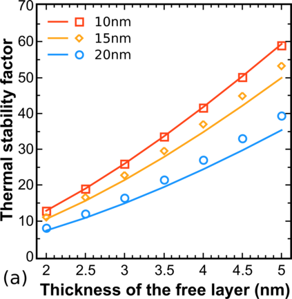
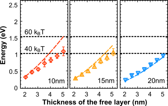
Now the thermal stability factor for the two types of the composite layer structures, C-MTJ and C2-MTJ, are compared. Figure 7.24a confirms that the replacement of the free layer consisting of the two half-ellipses separated with a narrow gap (C-MTJ) by only two small ellipses (C2-MTJ), does not result in a loss of thermal stability. With 52.5 × 10nm2 cross-section and 5nm thickness of the free layer a thermal stability factor ~60k BT is obtained.
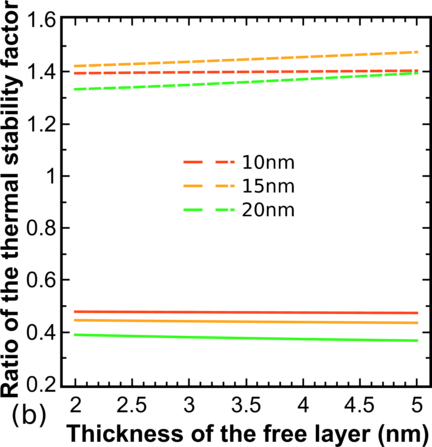
Next, the thermal stability factor for C2-MTJ with that of the two structures with monolithic free layer, conventional MTJ and M2-MTJ, are compared. Due to the removal of the central region from the monolithic structure the shape anisotropy in the C2-MTJ is decreased together with the thermal stability factor (Figure 7.24b). The constant ratio of the thermal stability factor as a function of the aspect ratio and thicknesses of the free layer indicates that the thermal stability factors for both structures scales similarly. This means that in order to increase the thermal stability factor in C2-MTJs it is sufficient to increase the thickness of the free layer and/or the aspect ratio.
In comparison to the second structure with monolithic free layer, M2-MTJ, the C2-MTJ structure shows a gain in thermal stability by a factor of ~2 times (Figure 7.24b), while maintaining the same switching time (Figure 7.22b), confirming the superiority of the C2-MTJ structure over the M2-MTJ one.
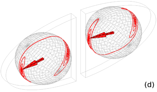
To determine the reason of the fast switching in C2-MTJs the switching process was investigated in detail. Figure 7.25 shows that, as in a C-MTJ, the switching processes of the left and right part of the C2-MTJ free layer occur in opposite senses to each other. Importantly, the switching occurs in the x-y plane. This is clearly seen at the time instance for 1.9ns, when the left and right ellipses pass simultaneously through the state (0; -1; 0) and (0; 1; 0) respectively (Figure 7.25).
In the following the height of the thermal energy barrier is compared with that of the switching energy barrier. As expected from the analysis of the magnetization dynamics, the switching barrier becomes practically equal to the thermal stability barrier in both C-MTJ (Figure 7.14) and C2-MTJ (Figure 7.26) structures. The C2-MTJ structure possesses a slightly lower switching barrier as compared to the C-MTJ structure with the same aspect ratio of the free layer.