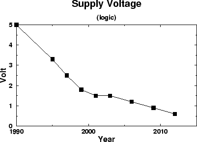
Equation (4.4) shows that the same capacitances have a negative influence on power consumption. Also, it stresses the main role of power supply voltage in this matter. While the initial voltage reductions, like the one from 5V to 3.3V, were mainly due to physical restrictions, they will be due to power consumption/dissipation limitations in the future. This is confirmed by the recent projections for the power supply voltages [2] shown in Figure 4.5. This trend seems to neglect adiabatic switching circuits [41] as an alternative technique to reduce power consumption.
We must note that voltage
reductions are also necessary to guarantee the reliability of devices. Lower
electrical fields are less a risk to the ever thinner oxides that come along
with scaling. Even if thicker gate dielectrics based on new materials
with dielectric constants greater than SiO![]() [42] will become usual, the
lower working temperatures (due to less power consumption of low voltage
technologies) will favor long device lives.
[42] will become usual, the
lower working temperatures (due to less power consumption of low voltage
technologies) will favor long device lives.
Although the demands on better interconnects and lower power supply voltages are inevitable, both will bring about severe modeling and technological problems that need to be solved. Classic parasitic extractors only assume planar capacitances and do not take into account fringing fields and other effects which are getting more and more important with technology scaling. At very high frequencies, packaging and bonding effects must also be studied.
The widely used SPICE level-3 model fails to describe devices in the moderate inversion regime [8]. In spite of that at power supply voltages as low as 0.6V weak and moderate inversion will gain a much higher importance than today. Although a large number of new models has been made available [43] they are either too specialized or too complex and difficult to calibrate (e.g. BSIM3v3 [44] has more than 100 parameters). The design of analog circuits will also render extremely complex as the dynamic range will be reduced. The Signal to Noise Ratio (SNR) will also be impaired.
Thermal management must be included in the design phase. This is a direct consequence of the expected high power that must be dissipated. Hot spots and temperature gradients in sensible parts of the chip (e.g. with analog circuitry) must be avoided. Modeling the packaging thermal behavior and cooler structures will be indispensable as well.
Some solutions to these and other related problems are given in the next part of this work. Using TCAD tools, the next chapter present a method for rigorous simulation of circuits fabricated in deep submicron technologies. We focus on two-dimensional device modeling and circuit simulation. In Chapter 6 we tackle the characterization of interconnect parasitics and thermal analysis of integrated circuits.