


Next: 5.2.2 Device Simulation
Up: 5.2 Application Example
Previous: 5.2 Application Example
5.2.1 A Low-Voltage, Low-Power Technology
To demonstrate the abilities of the described tools, they were used to
develope an advanced CMOS process. It is based on an twin well technology
with trench isolation and a  transistor's channel length. Careful
channel engineering allows to
reduce short channel effects and a TiN barrier layer is used to make
a reliable contact to the shallow source/drain junctions.
transistor's channel length. Careful
channel engineering allows to
reduce short channel effects and a TiN barrier layer is used to make
a reliable contact to the shallow source/drain junctions.
Only two metal layers are simulated, but this number could be extended
typically to six. The vias use a tungsten pad layer. The not
shown metal levels could be formed
in the same way as METAL2, but a CMP process step should be done to
smooth the oxide surface prior to metal deposition. This would usually be
necessary in the lowest ones, as normally the design
rules of the upper layers are quite large (they are used as power
distribution).
In Figure 5.3 the simulation flow controller
for hierarchical and user-friendly process recipe edition is displayed. The
simulated circuit is a 5-stage ring oscillator the layout of which is shown in
Figure 5.15. For the two-dimensional process simulations a
cut over the last inverter was performed (see also
Figure 5.15). This circuit though simple, contains
the most important
elements in a CMOS integrated circuit: Both PMOS and NMOS transistors and
the isolation structure between them.
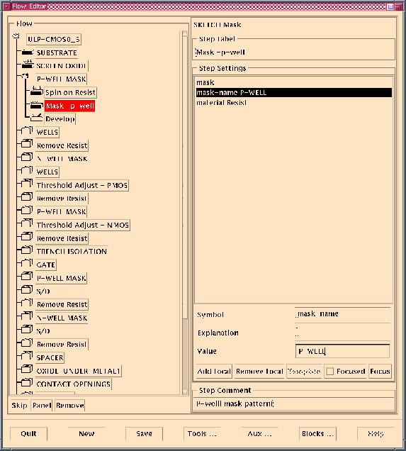
Figure 5.3:
The simulation flow controller: Specification the use of layout
layer P-WELL as mask for the P-well high energy implant.
 |
The most relevant
intermediate results from the simulation flow are shown in
Figures 5.4 to 5.11. Note that
the x-direction in these results
is not the same as in the layout of Figure 5.15. The
x-direction in the two-dimensional simulations has not layout
based coordinates, but refers to distances to the first point of the
cut-line. So whatever the direction of the cut, the results will
be in the x-axis for mask ticks and y-axis for depth (direction
perpendicular to the wafer plane).
Figure 5.4:
Substrate material: p-type (100)-oriented silicon (the picture
also shows a 40nm screen oxide layer formed afterwards).
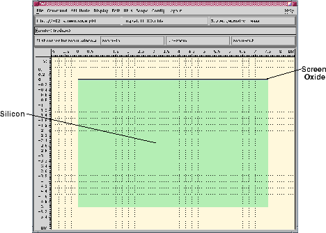 |
Figure 5.5:
N-well and P-well implants after annealing.
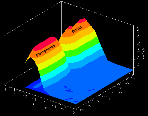 |
Figure 5.6:
Net-doping profile after threshold adjustment implants (the
simulation grid is also shown).
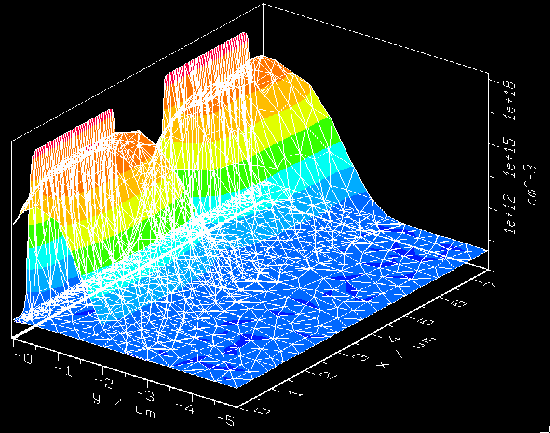 |
Figure 5.7:
Net-doping profile after trench etch with reactive ion-etching
and channel-stop implants.
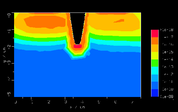 |
Figure 5.8:
Geometry after gate oxidation, gate polysilicon deposition
and sidewall spacer formation.
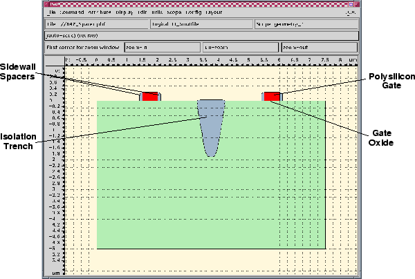 |
Figure 5.9:
Net-doping profile after source/drain implants.
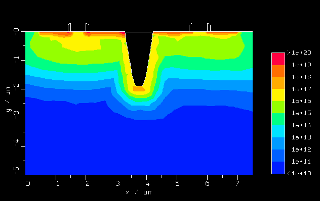 |
Figure 5.10:
Geometry after oxidation, contact hole etch, first metal
deposition and etching
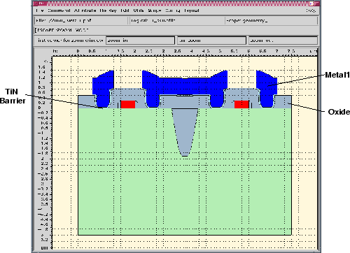 |
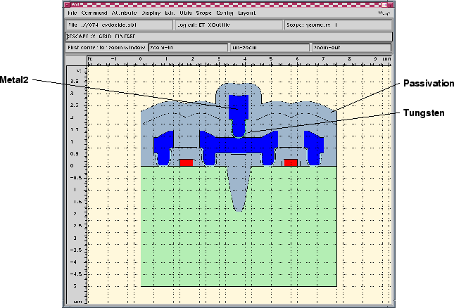
Figure 5.11:
Structure (final) after intermetal oxide deposition,
via hole etch, second metal deposition, second metal etching and
passivation.
 |
Next: 5.2.2 Device Simulation
Up: 5.2 Application Example
Previous: 5.2 Application Example
Rui Martins
1999-02-24