 |
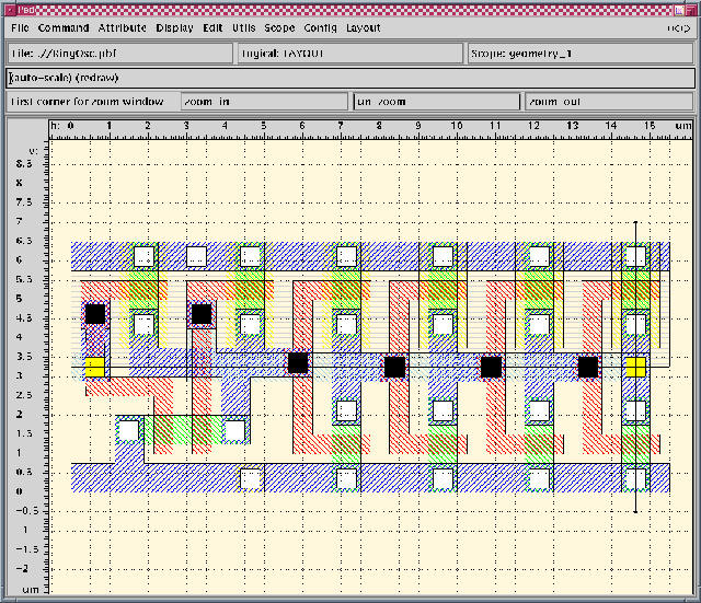
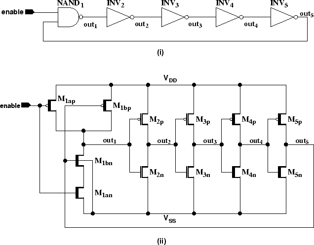
The layout corresponding to the schematic of
Figure 5.14-(ii) uses typical 0.5![]() design
rules and it is presented in Figure 5.15. To
save chip area all PMOS and NMOS transistors lie in the same
N-well or P-well, respectively. The feedback line is layed in METAL2
over the transistor.
design
rules and it is presented in Figure 5.15. To
save chip area all PMOS and NMOS transistors lie in the same
N-well or P-well, respectively. The feedback line is layed in METAL2
over the transistor.
Before we present the results of this circuit, we want to stress the importance of the possibility of checking the influence of technology parameters in the circuit performance. When the devices are defective due to a wrong fabrication setup, most probably a circuit like the ring oscillator will not work properly, i.e. it will not oscillate, the oscilation amplitude is to low or the frequency is lower than expected. For the initial tests on devices and circuits the inverter (in spite of being the simplest circuit) is a very good choice.
When developing a low-voltage, low-power technology for digital circuit
purposes, the most important issue is perhaps to achieve the highest
![]() current ratio145#3. This involves a careful
investigation of the optimal threshold voltage and proper process
parameters control: a too high threshold
voltage will reduce
current ratio145#3. This involves a careful
investigation of the optimal threshold voltage and proper process
parameters control: a too high threshold
voltage will reduce ![]() but also
but also ![]() and the devices will be
very slow. On the other hand, the option for a too low threshold voltage
can make
and the devices will be
very slow. On the other hand, the option for a too low threshold voltage
can make ![]() so large, that a proper operation of the device is not
possible.
so large, that a proper operation of the device is not
possible.
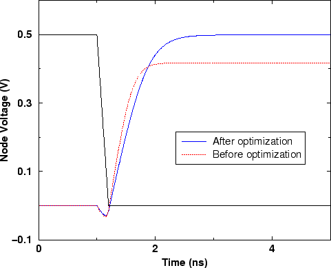 |
In Figure 5.16 we show the response of an inverter (like
the ones in the ring oscillator) for a case before the optimization of the
threshold adjustment implant and for the final devices (after optimization). It
can be observed that although the inverter operation is still achieved,
the output before optimization never reaches the power supply voltage. This
behavior could not be tolerated in a circuit, as the noise margins
are seriously reduced, even if its speed is a little faster than in the
optimized case. The problem was related to the too low value of the NMOS
threshold voltage that originated a large leakage current which,
associated to a relative low drive current of the PMOS transistor, forced
the output voltage to be somewhat below the upper power supply rail. Even
if ![]() of the PMOS transistor were enough, the circuit would have an
unacceptable high static power
consumption. After optimization, we end up with the device
characteristics shown in Table 5.1. The threshold
voltages as usually defined for transistors working in strong
inversion do not apply to these low-voltage technologies. The
threshold values reported in the following table are defined as the
gate-source voltage (with bulk and source connected) that
satisfy (5.1) [50].
of the PMOS transistor were enough, the circuit would have an
unacceptable high static power
consumption. After optimization, we end up with the device
characteristics shown in Table 5.1. The threshold
voltages as usually defined for transistors working in strong
inversion do not apply to these low-voltage technologies. The
threshold values reported in the following table are defined as the
gate-source voltage (with bulk and source connected) that
satisfy (5.1) [50].
| PMOS | NMOS | |
| |
0.5 V | 0.5 V |
| |
0.25 V | 0.25 V |
| |
16.5 |
25.5 |
| |
2.8 |
0.7 |
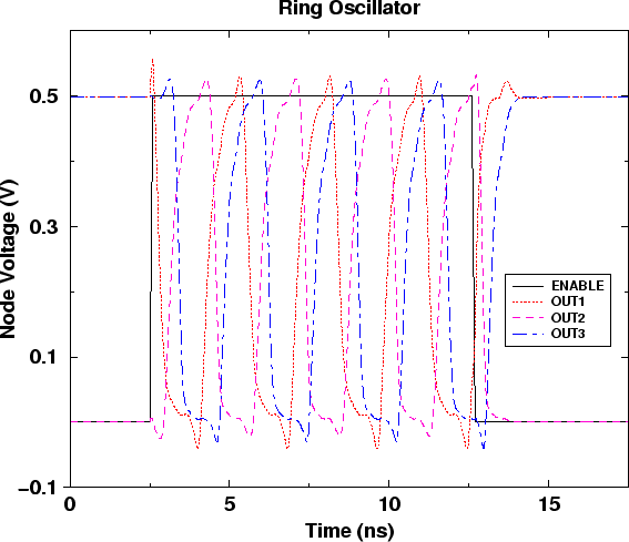
The result from the ring oscillator transient simulation is shown
in Figure 5.17. The delay as given by
(4.7) is 0.275![]() corresponding to an
oscillation frequency of 365MHz. In fact, there is a small
inaccuracy in using (4.7) because the
delay time in the NAND gate is slightly larger than in the
inverters (about 7.5%). This happens due to the reduced transconductance
of the series connected NMOS transistors (M
corresponding to an
oscillation frequency of 365MHz. In fact, there is a small
inaccuracy in using (4.7) because the
delay time in the NAND gate is slightly larger than in the
inverters (about 7.5%). This happens due to the reduced transconductance
of the series connected NMOS transistors (M![]() and M
and M![]() of
Figure 5.14-(ii)) in the NAND gate.
of
Figure 5.14-(ii)) in the NAND gate.
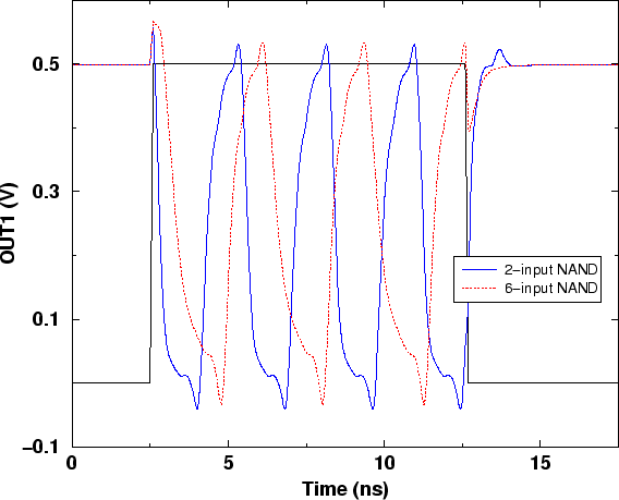
Although this effect also takes place in conventional CMOS technologies, it is
worsened here due to the lower drain-source transconductance of the devices in
the active region. This
is a severe limitation in
using complementary CMOS logic gates with many input variables. This
can be seen in Figure 5.18, where a ring
oscillator with the NAND of Figure 5.14
replaced by a 6-input NAND gate is simulated (all
but one input - used in the feedback path - are
connected to ![]() ). We can see a strong degradation in the
switching speed (in the fall time) due to the 6-input NAND gate.
). We can see a strong degradation in the
switching speed (in the fall time) due to the 6-input NAND gate.
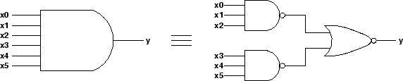
One solution is the decomposition of functions with a large number of input variables, into simple sub-functions as in Figure 5.19. But the optimal solution is not trivial as, in turn, delays due to interconnections arise. The extra parasitic interconnect capacitances will also become an extra load that can slow-down the individual gates switching times. Only detailed simulations can determine the best design choices.