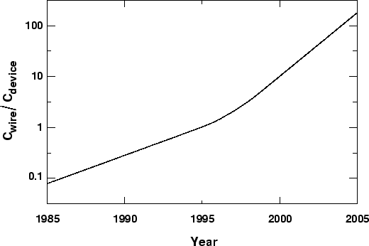
Down scaling the active devices played a major role in the achievement of these goals in the past but, as we have demonstrated in Chapter 4, the constraints for circuit speed and complexity are getting more and more governed by the interconnections between them. This trend can be clearly seen in Figure 6.1, as the total capacitance in internal nodes is becoming dominated by wiring. Moreover, recent generations of Application Specific Integrated Circuits (ASICs) include both digital and analog parts, which are very sensitive to crosstalk, noise coupling and other factors strongly dependent on routing. Even in pure digital high performance circuits, where the GHz regime will be reached very soon, the capacitive coupling between parallel data buses is creating formidable interference problems which can not be accurately described by simple models. At last, the ever increasing length of global interconnection wires makes RC delays getting worse.
The usage of advanced materials to improve in-circuit interconnections is not a long term solution. It may postpone these drawbacks, nonetheless, the physical limits will be reached soon [52]. The use of copper as conductor material for interconnect wiring (already utilized in very recent technologies [53]) will improve the resistance (in relation to aluminum) by 35%. The utilization of low-k dielectrics, such as MSQ [52], Xerogel [53] and HSQ [54] allows a reduction of 25% to 50% in the parasitic capacitances. However, as these materials suffer from poor adhesion and low thermal stability, they are not the ideal solution. Lowering the temperature also improves interconnects as lattice vibrations are slowed down. But even if no superconductor temperatures are used, this is an impracticable solution for desktop equipment as the cost and space requirements are too high. Another discussed technology is based on optical interconnections. Despite having an enormous potential, there are too many difficulties that will preclude it from being a solution for in-chip interconnections in a short/medium time scale.
The best solution to reduce parasitic interconnect effects is achieved by forcing design strategies with more aggressive design rules that compete with device scaling. This requires the abandon of conventional scaling rules in interconnections, where only lateral dimensions are shrunk while vertical sizes remain unchanged [55]. But scaling-down in the vertical direction is also dangerous. The resistance of wires increases and current densities get higher. Hence, the reduction of the capacitance of the wires is compensated by an increase of their resistance. Depending on the length of interconnections two cases must be considered: for local or inter-block interconnections the load is more important and the delay will be improved; for long distance interconnects where the RC product will remain constant or suffers even a small increase, this scaling must be accompanied by auxiliary techniques like the introduction of repeaters in the appropriate places. The increase in current density can also pose reliability problems, therefore, finding the optimal oxide thickness, wire width and minimum pitch distances between them, is not a simple task and the design of interconnect structures requires much more attention and new tools which accurately model all associated effects.
The recent back-end topography TCAD simulators are gaining importance once they are appropriate for the passive/parasitic device modeling, namely interconnection elements [56]. The three-dimensional structures created with topography simulators for complex deposition, etching and CMP processes, can then be used to predict the electrical characteristics of interconnects. This allows at an early stage of the design, the prediction of the behavior of the interconnect structures, that is, the design for interconnectivity.
This chapter describes a set of layout-driven CAD tools which perform interconnect analysis where the automatically created three-dimensional structures are derived from accurate topography simulation. We describe topography simulators, capacitance/resistance extraction programs and the linking between both. As temperature changes the electrical resistance of materials, temperature distributions are also calculated. This study is also important to verify the reliability of interconnects, as phenomena like electromigration are closely related to temperature.