 |
Resistance calculations were done with similar methods. As for uniform thickness layers the resistance of a square is always constant, the total resistance between two contacts is the number of squares between those points multiplied by the sheet resistance. Once more, the Layout Parameter Extraction (LPE) tools assumed that the fabricated wires exactly follow the layout.
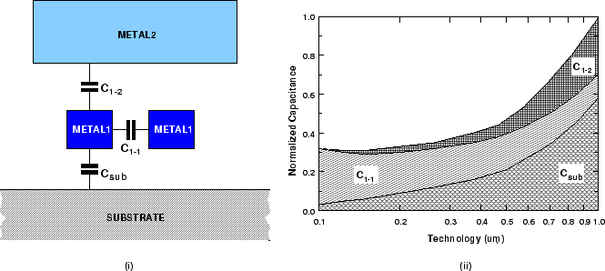
In modern technologies these methods can produce likely false results, because the parallel plate capacitor model cannot be used and the wire thickness is not constant. As Figure 6.2 shows for the capacitance case, the fringing effects must be equally considered and, in fact, the trend is that they will dominate.
This figure also shows that without scaling in the vertical design, the total
wiring capacitance will even start to increase slightly at 0.15![]() technologies. Although C
technologies. Although C![]() and C
and C![]() at this point are almost
negligible, the capacitance between adjacent wires at the same metal level
will cause this behavior due to the small pitch distance.
at this point are almost
negligible, the capacitance between adjacent wires at the same metal level
will cause this behavior due to the small pitch distance.
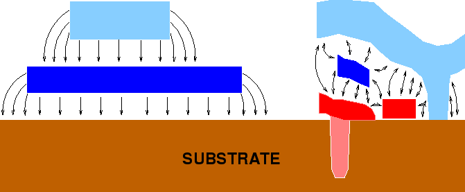
The example presented in Figure 6.2 is, yet, over-simplified as the metal wires cannot be considered planar and regular as depicted. This is becoming more acute, as new processes use multi-level metalization steps, trench etching and other methods that cause highly non-planar topographies as in the right part of Figure 6.3. Besides, the etching slope of the wires makes them highly irregular and they do not closely follow the layout because of lithographic phenomena that must be considered. Finally, although Figure 6.2 and Figure 6.3 are two-dimensional cuts, it should be made clear that due to the arbitrary form of interconnects, they in general will not have any axis of symmetry and only three-dimensional simulators can give accurate results.
 |
Several software packages were reported to extract capacitances and resistances in three dimensions. They can be roughly classified in terms of accuracy and range of applicability (i.e. the maximum size of the simulation domain) as follows:
In this work the main interest is in obtaining the maximum accuracy, so it focuses on tools belonging to the last group. Besides high accuracy, these methods allow an interaction between process parameters and circuit layout, in other words, between front-end and back-end design, that is necessary for global circuit/technology optimization. Traditionally, this goal is impaired by the data needed as input to these tools because the data formats change widely and the input processes are usually extremely time consuming and error prone (eg. geometry-based input formats entered manually). This restricts their use to simple problems (even if their solvers are powerful and in theory able to handle much larger problems).
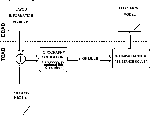
This solution requires a general approach, one that provides an interface between mask-layout, fabrication process and the extraction tools [63], [64]. Additionally, the result should be a circuit-level electrical model, compatible with standard circuit simulators as SPICE. In such a solution the structures under investigation are generated automatically, allowing ECAD designers to predict the interconnect behavior before any silicon is actually produced.
This way the conservative design rules of a conventional VLSI circuit design, where the design and fabrication phases are uncorrelated, can be relaxed and the goals initially formulated achieved: more compact circuits with improved performance and functionality, yet keeping good yield capabilities. A solution can be obtained by linking accurate etching deposition (and other) topography simulators available in TCAD environments with parasitic extractor tools and layout. This constitutes a large improvement over the tools presented in [63], [64], as they use too simple models to simulate the chip topography. The data-flow of the proposed tools is shown in Figure 6.4.