For non complex cases, simple rules can be used to derive the three-dimensional model from the layout. The easiest (and fastest) method is projecting the binary layout masks (with optional inclusion of lithographic effects as explained in Section 3.4) into the direction perpendicular to the wafer surface by some thickness. With this method each generated segment is completely planar regardless of what lies underneath. To avoid this drawback, a conformal representation was proposed [64]. Here, the thickness of the resulting segments is also constant, but the same applies to the oxide (or other dielectric) thickness between them. Thus, the upper topographies ``jump'' when a wire is crossing below. Without adding too much complexity, this result is closer to the real situation and increases the quality of the results.
A more accurate technique consists in merging the methods mentioned above with two-dimensional simulation profiles [65]. This assures a better degree of accuracy in the structure's solid model, but cannot handle three-dimensional effects on corners. This is a severe problem in local interconnects and other structures with highly irregular shapes, where only fully three-dimensional simulations can give precise results.
We use the topography simulator etch3d [66] to create highly-realistic solid models of integrated circuit interconnections. This program uses methods based on morphological operations derived from image processing, which are performed on a cellular material structure where the formation of unphysical surface loops is completely avoided.
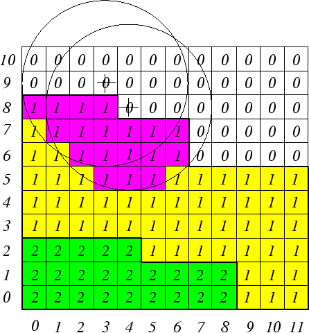
In the cellular format, materials are represented as a three-dimensional array of cubic cells (or an array of squares for the two-dimensional case). Each cell refers to a different material identified by a 7-bit index (0 corresponds to vacuum) as in Figure 6.5 and a 1-bit etch/not-etched flag. In that figure we also show a circle, the so-called structuring element, which controls the local etching or deposition rates according to its spatial dimensions. The structuring element is a circle for isotropic etch/deposition steps (see Figure 6.5) with a radius proportional to the etch/deposition rate. For non-isotropic operations an ellipsis with a constant ratio between the major and minor axis is used for defining the degree of anisotropy. The same considerations apply to the three-dimensional case where the circle and ellipse are replaced by a sphere and an ellipsoid, respectively.
The structuring element is moved along the surface boundary and cells are added if a deposition step is performed or removed in the etching case (these operations are only performed over cells laying inside the structuring element). The surface boundary is easy to determine: It consists of material cells which are adjacent to vacuum cells.
 |
For reactive ion etching and sputter deposition the visibility of the particle source seen from the position of the structuring element is needed as it influences both the local surface velocity, the size, shape and orientation of the ellipsoid. This causes the simulation of such processes to be slow if fast algorithms are not used. For more information about these simulators and topography simulators in general consult [66]. Optimized implementations of the cellular based algorithms are presented in [67].
The simulator etch3d has an auxiliary tool for easily defining patterning steps. This tool uses the layout environment described in Chapter 3 to provide a common user-interface. To avoid the necessity of redundant layout layers, a combination of layers can be specified using boolean operations in the patterning procedures. This allows the layouts, for example, to have only one CONTACT layer that is used for both source/drain and gate contacts. For the first case one should use CONTACT && ACTIVE-AREA && METAL1 and CONTACT && POLY1 && METAL1 for the latter. The simulator covers the following topographic processes: