The most intuitive meshing procedure consists in the extraction of solids from the material interfaces and the subsequent use of a fully unstructured three-dimensional grid. However, extracting solids from the material array is not trivial, because the solids obtained in such a way have a very irregular surface with a high number of points, which causes many problems to a gridder. This problem can be solved by applying a low-pass filter on the structure's surface, prior to gridding. Yet, this operation is not readily realizable and other methods were investigated. We analyzed the possibility of using the same laygrid program on structures created by etch3d, as that tool is very stable and robust (specially with the triangle option). The way how it was realized is explained next.
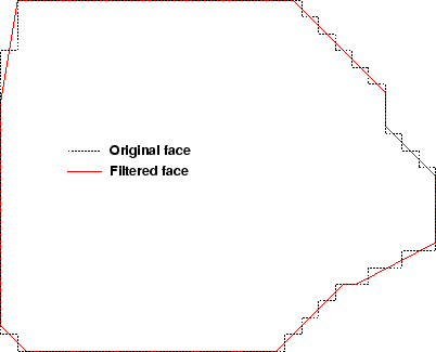
One plane of the three-dimensional array of the cellular material representation can be considered as a bitmap image, where the color of each pixel corresponds to the material index of the cell. If we apply an edge detection algorithm to this image, polygonal faces defining material boundaries are found and used to build one layer for the laygrid preprocessor, in the same way as the layout was used. The faces can easily be smoothed by removing non-important points from the typical stair patterns coming out from the cellular data (in opposition to the difficulties in the three-dimensional case). As Figure 6.9 demonstrates, a large degree of simplification can be obtained. The 36 points of the original face were reduced to only 12 without introducing any error in the actual geometry.
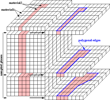
To generate a complete structure, the array is sampled in the vertical direction and a new layer is inserted if the difference between the actual image and the last that has been inserted is larger than an error criterion. In Figure 6.10 we show the polygonal faces obtained at the boundaries between two materials in non-uniform sampled planes.
As the number of grid nodes and consequently the memory and time consumption
for the following simulations increases with the number of inserted
points, the sampling must be performed efficiently. Approaches with
simple algorithms based on an overall error over the image were
not satisfactory because they tend to ignore small feature details. The
following algorithm successfully overcame this problem.
 |
This way, a three-dimensional structure is created and gridded in a form compatible with the subsequent tools. The main advantages of this approach are the simplicity and robustness. A drawback is that it generates more grid points than necessary if the structures contain large variations in the vertical direction. This is compensated by easily allowing the construction of structures that are partially derived from topography simulation and partially created directly from the layout (saving grid points).
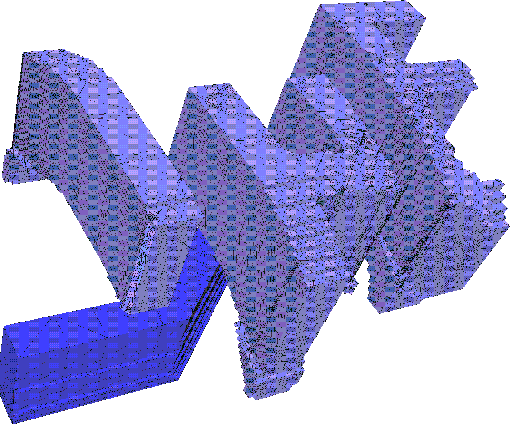
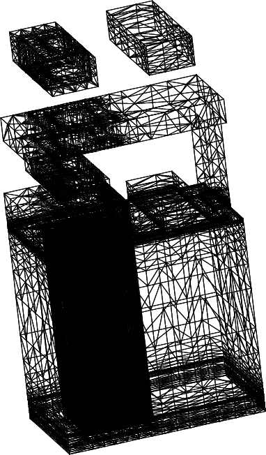
Applying the described algorithm to the ![]() -logo example we obtain the solid
model and grid of Figure 6.11 and
Figure 6.12. For the topography simulation we used
anisotropic etching of aluminum and isotropic SiO
-logo example we obtain the solid
model and grid of Figure 6.11 and
Figure 6.12. For the topography simulation we used
anisotropic etching of aluminum and isotropic SiO![]() deposition. The thickness
of the aluminum wires and SiO
deposition. The thickness
of the aluminum wires and SiO![]() is the same as specified
in Figure 6.6.
is the same as specified
in Figure 6.6.
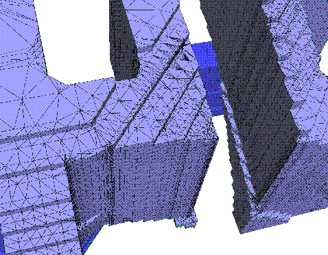
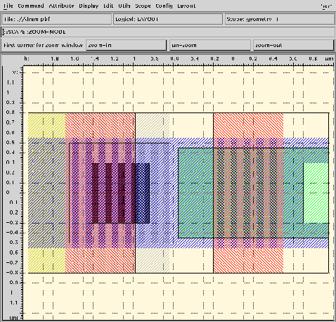
In Figure 6.14 a more complex
example is presented. It consists of a deep trench DRAM cell where the capacitor
is formed by topography simulation and the poly-gate and metal lines are
obtained directly from the layout of Figure 6.13. The
bottom part of the
capacitor was created so as to avoid sharp edges at the corners, which may
lead to the formation of a thinner oxide layer there. As a high electric field
will emerge in these regions, a too large leakage current could
occur [71]. In order to round the corners, an oxidation and stripping
step was carried out before forming the actual SiO![]() dielectric film. As
this film is only
dielectric film. As
this film is only ![]() thin, a very large number of grid points are necessary
to resolve such small dimensions (as it is seen
in Figure 6.14), making
this a difficult problem and a good test of the capabilities of the tools. In
that figure the described adaptive sampling mechanism of Z-planes can
be observed as well.
thin, a very large number of grid points are necessary
to resolve such small dimensions (as it is seen
in Figure 6.14), making
this a difficult problem and a good test of the capabilities of the tools. In
that figure the described adaptive sampling mechanism of Z-planes can
be observed as well.