These exotic topographies can only be predicted with tools
capable of very accurate etching and deposition simulation. We checked ours
in the vertical stacked capacitor, one of the most commonly used electrode types
of this family. We simulated it as described in [88]. The
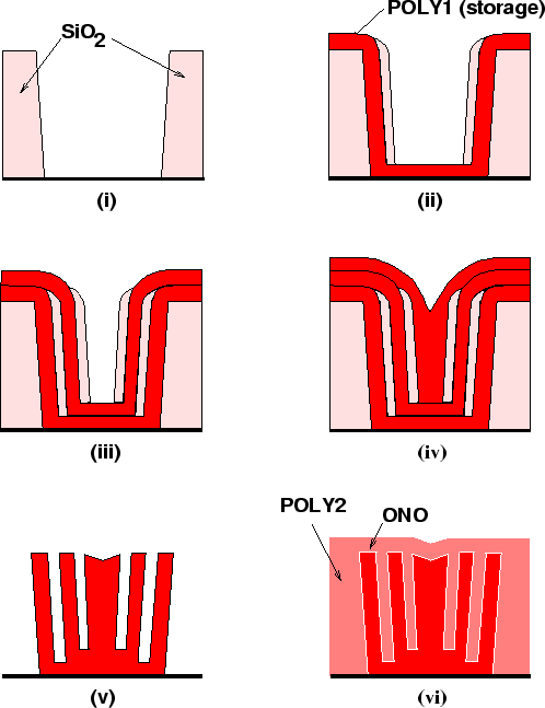
several stages in the process flow of the capacitor are shown
in Figure 7.6. It starts with trench opening in
a SiO![]() planar layer with a reactive ion etching process (i), followed
by isotropic deposition of POLY1 and SiO
planar layer with a reactive ion etching process (i), followed
by isotropic deposition of POLY1 and SiO![]() ,
etching back of
the SiO
,
etching back of
the SiO![]() with high directional rate (vertically) (ii) and the previous step
is repeated (iii). Then, the structure is
refilled with POLY1 (iv) and etched back to adjust the
height (v). Finally the oxide is removed, the dielectric (ONO) deposited
and filled with POLY2 (the plate node) (vi). The total diameter
is
with high directional rate (vertically) (ii) and the previous step
is repeated (iii). Then, the structure is
refilled with POLY1 (iv) and etched back to adjust the
height (v). Finally the oxide is removed, the dielectric (ONO) deposited
and filled with POLY2 (the plate node) (vi). The total diameter
is ![]() ,
the height 800nm and the wall thickness of the storage node
is adjusted to 80nm.
,
the height 800nm and the wall thickness of the storage node
is adjusted to 80nm.
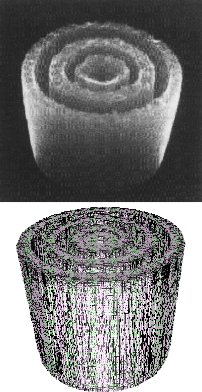
Figure 7.7-top shows a SEM after the storage plate formation - step (v) and the solid model (and grid) of the simulated structure is presented in Figure 7.7-bottom (only the elements of material POLY1 are shown). The total structure has 1 million elements, the extracted value is 26.1fF and it is in close agreement with the measured value of 23.3fF. Although the displayed structure exhibits almost cylindric symmetry a full three-dimensional simulation was performed. The total run time of the topography simulation is 27 minutes in a DEC 3000/400 workstation.
 |