![2e∑ [ iℏ ∂ ]
J(z) = - --- fα (k ∥)Re Φ⋆α(z)--⋆------Φα(z)
A α,k∥ m (z)∂z](diss_html179x.png)
Throughout this section we consider GaAs wells and barriers composed of AlxGa1-xAs.
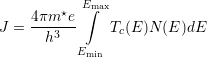
On the basis of the Robin boundary conditions (3.19) and (3.20) the current density is numerically evaluated for periodic QCL structures as well for quasi-periodic systems. The transport of charge through the structure arises as a property of the wave function, and the current density is expressed as [1]
|
| (6.1) |
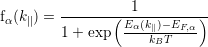
where A is the cross-sectional area of the quantum well structure. The work of P. Harrison [95] suggests that the electron distributions in both the active region and the injector subbands are thermalized and thus the energy distribution of electrons in each subband can be approximated by a Fermi-Dirac distribution function
 | (6.2) |
where EF,α is the quasi Fermi energy of the α-th subband and Eα(k∥) = Eα + ℏ2k∥2∕2m⋆.
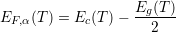
The electron states are evaluated using a selfconsistent Schrödinger-Poisson solver, where the electron concentration is related to the electronic wave functions and the electron sheet densities in the corresponding subbands which can be calculated according to the Fermi-Dirac distribution. For a given total sheet density the quasi Fermi level is obtained iteratively, where the initial value of the quasi Fermi level is taken to be [96]
 |
while the band gap in eV is
 |
with
 |
The conduction band edge is given by
 |
with
 |
The Tsu-Esaki Model describes the tunneling current density. The corresponding formula is usually written as an integral over the product of two independent parts which only depend on the energy component perpendicular to the interface [97].
 | (6.3) |
Tc (E) is the transmission coefficient which characterizes the penetrability of the considered energy barrier. The supply function N(E) describes the supply of carriers for tunneling.
Figure 6.2 compares the simulated current density using the Robin boundary condition approach with the current density calculated by the Tsu-Esaki model for a GaAs/Al0.3Ga0.7As Fibonacci superlattice (FSL) [98] which is a quasi-periodic multibarrier system. The generalized FSL is generated by an iterative process according to the Fibonacci sequence [99]
 |
where A and B are the blocks of the well and barrier. A special kind of FSLs with a higher quasi-periodicity follows the iteration rule [100]
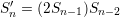 |
Table 6.1 presents a few initial generations of FSLs of the two different kinds.
The FSL type considered is S5′ which has the sequence BBABBABBBABBABBBA, where A and B
are the elementary blocks corresponding to the GaAs quantum well and the Al0.3Ga0.7As barrier,
respectively. The width of the well block is taken to be 5 unit cells of GaAs monolayers, whereas the
number of the unit cells belonging to Al0.3Ga0.7As monolayers for the barrier block equals to
3. The lattice constants for the well and barrier materials are 5.6533  and 5.65564
  ,
respectively. The appearance of resonance-type peaks in the current density curves is typical for
quasi-periodic systems, and the results obtained are in good agreement with the Tsu-Esaki
model.
,
respectively. The appearance of resonance-type peaks in the current density curves is typical for
quasi-periodic systems, and the results obtained are in good agreement with the Tsu-Esaki
model.
| n | Sn | Sn′ |
| 1 | A | A |
| 2 | B | B |
| 3 | BA | BBA |
| 4 | BAB | BBABBAB |
| 5 | BABBA | BBABBABBBABBABBBA |
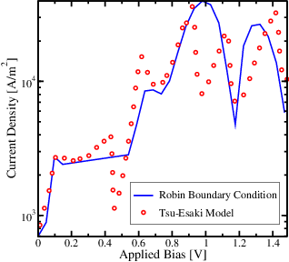
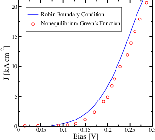
The ability of the Robin boundary conditions to produce satisfactory current carrying states is also verified by comparing our results for the tunneling current density with calculations based on nonequilibrium Green’s functions (NEGF) [1]. For this purpose a typical example of a midinfrared quantum cascade laser is considered [9].
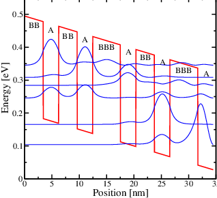
Figure 6.3 illustrates the conduction band profile of this device. The layer sequence of one period belonging to the GaAs/Al0.33Ga0.67As structure, in nanometers, starting from the injection barrier is: 5.8, 1.5, 2.0, 4.9, 1.7, 4.0, 3.4, 3.2, 2.0, 2.8, 2.3, 2.3, 2.5, 2.3, 2.5, and 2.1, where normal scripts represent the wells, bold the barriers.
The comparison of the obtained current-voltage characteristics with the simulation employing the nonequilibrium Green’s functions method is illustrated in Figure 6.4. The simulation is performed with the number of periods to be 30 and the temperature is taken to be 77 K. As in the case of quasi-periodic superlattices, the application of our method to calculate current carrying states proves to be very promising for periodic QCL structures as well.
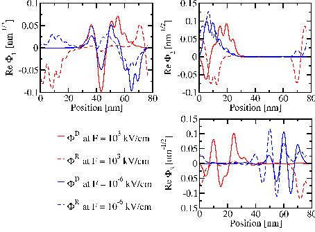
To illustrate the convergence of the solution to the Robin problem and the Dirichlet problem as Eα → ∞, we investigated the transformations of the wave functions as a function of the applied electric field, because the energy levels increase as the electric field decreases. For this purpose the real part of the wave functions belonging to the Robin problem are compared to the solutions of the Dirichlet problem. The imaginary part, indicating the development of the current carrying states, are studied analogously.
The order of magnitude we use for the electric field is 103 kV/cm on the one hand and 10-6 kV/cm for the weak field calculation. The investigated structure is the same three-level QCL design as above. The real components of the wave functions are plotted in Figure 6.5 for the electric fields F = 103 kV/cm and F = 10-6 kV/cm. For F = 103 kV/cm the calculations show obvious deviations in the spatial dependence between the solutions of the Robin and Dirichlet boundary value problems, unlike the weak field case F = 10-6 kV/cm, where a convergence between these solutions is observable.
The imaginary components of the wave functions corresponding to the Robin boundary value problem are plotted in Figure 6.6. At the very small electric field F = 10-6 kV/cm the imaginary part is almost zero everywhere except some very small peaks whose magnitudes are insignificant compared to the imaginary part of the wave function at F = 103 kV/cm.
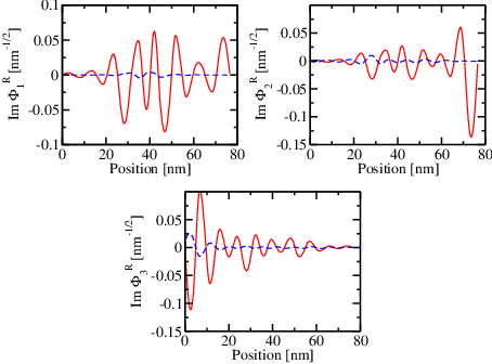
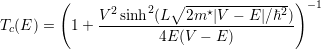
Since the imaginary part of the wave function becomes zero with increasing energy, our results indicate that the tunneling current vanishes in this case. This behavior can be understood in terms of the transmission coefficient which expresses the probability of tunneling and decays rapidly with energy according to [101]
 | (6.4) |
where Tc denotes the transmission coefficient for an electron in a heterostructure.
As mentioned above, the energy levels increase as the electric field decreases. Due to equation (6.4) the transmission coefficient decreases significantly with decreasing electric field, which is illustrated in Table 6.2. The three energy levels correspond to the upper and lower laser levels. Thus, by reducing the bias the conduction decreases and only minimal current flows. In this low field region the open boundary condition approach yields no significant deviation from the Dirichlet boundary value problem.
| F | E1 | E2 | E3 | Tc(E1) | Tc(E2) | Tc(E3) |
| 103 | 9.7 | 11.4 | 24.4 | 0.683 | 0.721 | 0.787 |
| 10 | 31.5 | 49.8 | 67.8 | 0.524 | 0.611 | 0.672 |
| 10-2 | 72.3 | 94.7 | 118.2 | 0.337 | 0.375 | 0.384 |
| 10-6 | 114.6 | 138.8 | 169.3 | 0.118 | 0.133 | 0.171 |
Here, we focus on the calculation of optical gain under consideration of the proposed Robin boundary conditions. Due to the strong dependence of the dipole matrix element on the wave function the determination of optical gain qualifies for verification of boundary conditions.
In QCLs intersubband transitions contribute to the gain profile, especially the transitions between the upper and the lower laser level. In general, the standard expression for optical gain in semiconductors can be written as [102]
![πe2ℏ 2 ∫
g(ℏω ) = n-ϵcm2-ℏω-|Mu,l| ρ [fu(E )- fl(E )]Λ (ℏω)dE
0 0](diss_html199x.png) | (6.5) |
Here, f(E) denotes the distribution function for the electrons. |Mu,l|2 represents the transition matrix element, ρ is the density of states, and Λ is the lineshape function. In a quantum well, the density of states can be taken as ρ = m⋆∕πℏ2L [103] and the transition matrix element is approximated by the dipole matix element according to Mu,l = m02ω2|zul|2. Substituting these approximations for the density of states and the dipole matrix element, and using the line shape as proposed in [104]
![Λ(ℏω) = -----γ(E-)∕π-----
[ℏω - E ]2 + γ2(E )](diss_html200x.png) | (6.6) |
the optical gain can be estimated as [105]
![∫∞
e2|zul|2m-⋆ω- -ℏγ-(E-)[fu(E-)--fl(E-)]-
g(ℏω) = ℏ2cnrϵ0L dEπ [ℏω - E ]2 + [ℏγ(E)]2
0](diss_html201x.png) | (6.7) |
where zul is the dipole matrix element, nr is the refractive index, ϵ0 is the vacuum permittivity and c is the speed of light. The dipole matrix element depends strongly on the wave functions of the relevant states, and so does the optical gain.
The validity of equation (6.7) is not restricted to any particular scattering mechanism. Certain assumptions have to be made about γ. We assume that the homogeneous broadening γ is dominated by the interaction with optical phonons [106]. Thus
The top line describes optical phonon absorption and the bottom line optical phonon emission, where γ0 = (πe2 ∕2ℏ)[1∕ε∞- 1∕ε0]qph, qph = (2meωph∕ℏ)1∕2, and the phonon occupation number is given by Nph = 1∕(exp (ℏωph∕kBT) - 1). Furthermore, εs and ε∞ are the low and high frequency dielectric constants respectively.
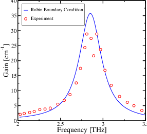
We consider a laser consisting of 90 periods of a GaAs/Al0.15Ga0.85As heterostructure at a temperature of 70 K [107]. The GaAs/Al0.15Ga0.85As layer sequence in nanometers is 3.8, 14.0, 0.6, 9.0, 0.6, 15.8, 1.5, 12.8, 1.8, 12.2, 2.0, 12.0, 2.0, 11.4, 2.7, 11.3, 3.5, and 11.6, where the AlGaAs layers are in bold. Figure 6.7 shows our simulation results to be in good agreement with measurements that are performed on this QCL design [108].
The dipole matrix element between states Ψα and Ψβ along the well growth direction z is given by [109]
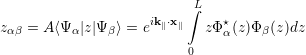 | (6.8) |
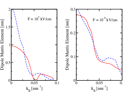
In order to obtain numerical illustrations for zαβ = ei2πk∥∕k∥max ∫ 0LzΦα⋆(z)Φβ(z)dz, the product |x ∥ | cos(x∥,k∥) is set to 2π∕k∥max, and k∥max = 0.1nm-1. The calculations of the dipole matrix elements, which performed for the two different electric field strengths 103 kV/cm and 10-6 kV/cm, are illustrated in Figure 6.8 as functions of the wave vector k∥. The dashed curves represent the results determined taking into account Robin boundary conditions and the solid curves result from Dirichlet boundary conditions. A comparison of the results belonging to the different electric fields reveals that the solutions of the Robin and Dirichlet boundary value problems converge when lowering the electric field. Thus, our calculations demonstrate the accuracy of the proposed Robin boundary conditions for QCL simulations. However, for the unbiased case Dirichlet boundary conditions yield nearly comparable results.