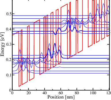
Figure 6.9: Calculated conduction band diagram and squared wave functions for a
GaAs/Al0.15 Ga0.85As QCL under an applied field of 10 kV/cm.
Using the Monte Carlo simulation scheme described previously, we have calculated the steady state carrier distributions and the current-voltage characteristics of a QCL in the THz region.
The structure considered consists of a combination GaAs wells and Al0.15Ga0.85As barriers [110]. The layer sequence of one cascade, in nanometers, is: 9.2,3,15.5,4.1,6.6,2.7,8,5.5, where normal scripts denote the wells and bold the barriers. Only the widest well is n-type doped with a low density of 1.8 × 1010 cm-2. Together with the squared envelope functions of the relevant bound states, the conduction band profile is plotted under an applied bias of 10 kV/cm in Figure 6.9.
The numerical values used for the relevant material parameters are listed in Table 6.3, where the difference in the electron affinity χe between the two materials determines the conduction band offset, and ϵS and ϵ∞ denote the static and high frequency dielectric constants. For the given GaAs/AlGaAs system, these values are well established and can be looked up in [111] and [112].
| GaAs | Al 0.15Ga0.85As | |
| m Γ⋆ | 0.067 | 0.075 |
| mX⋆ | 0.32 | 0.311 |
| ϵS | 12.90 | 12.47 |
| ϵ∞ | 10.89 | 10.48 |
| χe [eV] | 4.07 | 3.905 |
| ℏωLO [meV] | 36.25 | 35.30 |
| ρ [g/cm3 ] | 5.36 | 5.12 |
Eac [eV/ ] ] | 3.6 | 3.49 |
Eop [eV/ ] ] | 5.9 | 6.0 |
DΓX [eV/ ] ] | 4.1 | 5.2 |
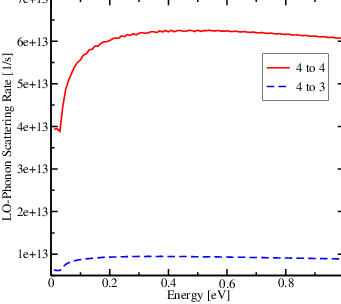
The optical transitions occur between the upper and lower laser states. The lower laser state is rapidly depopulated into the states 5′, 4′ or 3′ via LO-phonon emission. In order to enhance this process, the energy separation between these subbands should be close to the LO-phonon energy of the well material. Furthermore, the spatial overlap between the upper state and the lower state is kept as small as possible to increase the upper state lifetime. Figure 6.10 depicts the calculated LO-phonon rates 4 → 4 and 4 → 3. The energy of the initial states are given on the horizontal axis, and the zero energy reference value is taken at the bottom of subband 4.
Starting with a constant population initially assigned to each subband and using a constant time step of 5 fs we have monitored 10000 particles during 10 ps. Initially each subband has an equal number of particles, and subsequently the ensemble evolves until the simulation ends. After each time step the statistics are updated. The numerical model for the QCL structure studied includes five subbands per stage and periodic boundary conditions are imposed [113].
Electron-LO phonon, acoustic and optical deformation potential, and intervalley scattering are included in the simulation with the relevant scattering rates computed at a temperature of 70 K and stored for each subband pair for a discrete number of initial electron energies.
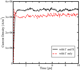
Figure 6.11 shows the time evolution of the current density with and without Γ-X intervalley scattering at an electric field of 10 kV/cm. It can be seen that the inclusion of intervalley scattering increases the current density indicating that the Γ-X electron transfer plays a significant role as a mechanism for depopulation of the lower laser level. In Figure 6.12, the obtained electron distributions of the individual subbands are depicted over the kinetic energy.
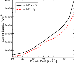
Figure 6.13 displays the obtained current density with and without X valley transport, where the range of the applied field is 10 to 70 kV/cm and the chosen calculation step is 5 kV/cm. The results demonstrate that for this QCL structure the inclusion of Γ-X intervalley scattering leads to an increase in the current flow. Without Γ-X electron transfer the results are up to 10 % lower.
The output characteristics of the Monte Carlo simulation show that the effect of intervalley
scattering processes is significant for the charge transport and not negligible in performance
investigations.
In this section, the impact of interface roughness scattering on the device performance is of
particular interest. Especially, we focus on the temperature sensitivity of the electron transport.
For this purpose, we take a look at the subband population and the current density as a
function of the temperature. Throughout the simulations, the characteristic height and the
correlation length of the interface roughness are taken as Δ = 2.83  and Λ = 70
  respectively
[114].
respectively
[114].
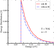
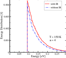
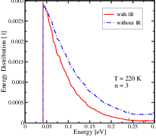
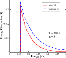
In Figure 6.14 and 6.15 we show the calculated electron distributions of the upper and lower subband for different temperatures. In general, the interface roughness scattering is found to be more dominant for higher temperatures. Moreover, it changes the occupation of the upper and lower laser levels significantly. We observe an increase in the occupation of the upper laser level due to interface roughness, while the occupation of the lower laser level gets reduced. The variations of the occupation due to rough interfaces increase with temperature, and for 300 K the variation can be as large as 27%, which illustrates their important influence on this THz QCL design.
In general, we observe a significant increase in the population of the upper laser level for higher temperatures, while the population of the lower laser level decreases somewhat.
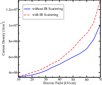
The effect of rough interfaces on the current voltage characteristics is illustrated in Figure 6.16 where the current density with and without interface roughness scattering is displayed. The temperature is taken as 70 K. Interface roughness scattering enables a better population of the upper levels and obviously increases the current density. Moreover, this effect gets more dominant for higher electric fields.
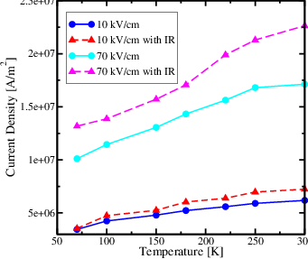
Figure 6.17 illustrates the dependence of the current density on the temperature for the considered THz QCL structure at different applied biases. In the case of F = 10 kV/cm, the inclusion of interface roughness scattering results in a significant impact only for higher temperatures. However, for F = 70 kV/cm the effect of rough interfaces is noticeable even for 70 K and increases with temperature.
The determined results demonstrate that interface roughness scattering plays an important role for the electron transport in THz QCLs. This mechanism introduces a significantly higher temperature sensitivity for the electron transport.
The simulator has been used to simulate a GaAs/AlGaAs MIR QCL structure and investigate the role of Γ-X intervalley scattering as a mechanism for the depopulation of the lower laser level, since a lot of interest arose for intervalley electron transfer in quantum well structures [115, 116, 117].
We propose to modify the Al content and the width of the collector barrier of the given QCL design in order to increase the overlap between the upper X-state of the next stage and the lower Γ-state of the central one.
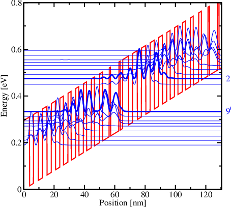
Figure 6.18 illustrates the conduction band profile under an applied field of 40 kV/cm. In the following, we will call this design structure A, where the layer sequence of one cascade starting from the collector barrier is, in nanometers [2]: 3.9, 2.6, 3.1, 2.8, 2.9, 2.9, 2.7, 2.9, 2.4, 2.9, 2.2, 2.9, 2.2, 3, 2, 3.2, 2, 3.5, 1.9, 4.3, 0.94, 5, 0.94, 5.4, 0.94, and 1.6. Normal scripts denote the GaAs wells and bold ones the Al0.45Ga0.55As barriers. The upper laser level is labeled 9, and the lower level is labeled 2.
The idea is to modify the collection barrier in a way that the Γ-X intervalley scattering mechanism can be used for an improvement of the device performance. Primarily, the intention is to increase the overlap between the lower Γ-state of the central stage and the upper X-state of the next stage. This is realized by modifying the width and the Al content of the collector barrier. In the following, the modified design will be called structure B.
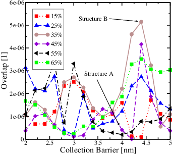
Figure 6.19 shows the overlap between the lower Γ-state and the upper X-state of two adjacent stages for different Al contents and collector barrier widths. Regarding structure B, these results suggest to set the collector barrier width to 4.5 nm and the Al content to 35 %.
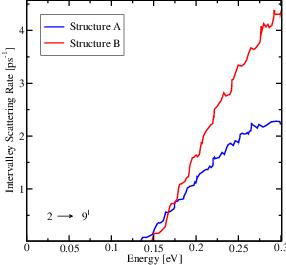
Applying these modifications, the determined Γ-X intervalley scattering between the lower state 2 and the upper state 9′ of the next stage increases significantly. Figure 6.20 illustrates this circumstance by showing the corresponding scattering rate for structure A and structure B at an electric field of 40 kV/cm.
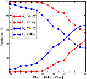
In Figure 6.21, the variation of the electron population in the Γ and X valleys with the electric field is presented. By comparing the trends of structure A and structure B, one can observe that the X-valley electron population increases with the field, where the increase is obviously higher for structure B.
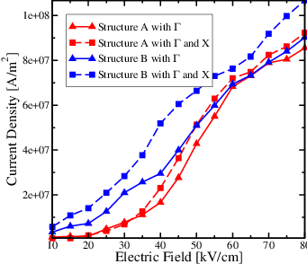
Our results indicate a significant increase in current density when considering Γ-X intervalley scattering for the modified structure B, whereas structure A shows negligible deviations. Figure 6.22 shows the obtained current densities for both structures in dependence on the electric field and highlights the importance of intervalley charge transport for QCL design considerations [118].
Since design modifications in terms of optimizing the overlap cause a crucial change in charge transport properties, it is obvious that the inclusion of X-states in the QCL dynamics introduces a new degree of freedom in the engineering of intersubband devices.
Here, a comparison of simulation results with experimental measurements for a recently developed InGaAs/GaAsSb QCL is presented. Aluminum-free QCLs are of big interest, since these structures do not suffer from degradation owing to the oxidation of aluminum during the fabrication process and laser operation [119]. Furthermore, aluminum-free structures are resistant to dark-line defects [120], which are responsible for abrupt failures in GaAs/AlGaAs lasers. A promising candidate for an aluminum-free QCL is the InGaAs/GaAsSb material system where the electron effective mass in the GaAsSb barriers is 0.045 m0. Compared to common QCL barriers such as AlGaAs and InGaAs, this effective mass is low and results in the growth of thicker barriers which are less sensitive to thickness fluctuations [121, 122, 123]. This is the notable advantage of InGaAs/GaAsSb structures compared to designs containing aluminum.
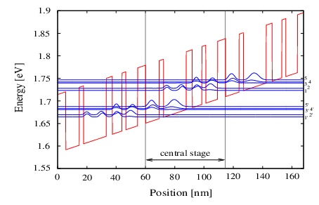
Figure 6.23 illustrates the conduction band profile for the considered QCL under an applied bias of 30 kV/cm. The layer thicknesses of the In0.53Ga0.47As/GaAs0.51Sb0.49 structure starting from the injection barrier are, in nanometers [3]: 8.1, 2.7, 1.3, 6.7, 2.2, 5.9, 7.0, 5.0, 1.9, 1.2, 1.9, 3.8, 2.7, 3.8, 2.8, 3.2. The barriers are in bold, and the underlined layers are Si doped (4 × 1017 cm-3). The fabricated QCL is 60 μm wide and 2 mm long.
Table 6.4 shows the numerical values for some relevant material parameters. These standard values can be looked up in the literature [124, 125, 126, 127, 128, 129].
| In 0.53Ga0.47As | GaAs0.51Sb0.49 | |
| m Γ⋆ | 0.043 | 0.045 |
| mX⋆ | 0.279 | 0.26 |
| ϵS | 13.90 | 14.30 |
| ϵ∞ | 11.60 | 12.64 |
| χe [eV] | 4.06 | 4.46 |
| ℏωLO [meV] | 34 | 33.20 |
| ρ [g/cm3 ] | 5.50 | 5.45 |
Eac [eV/ ] ] | 6.4 | 5.7 |
Eop [eV/ ] ] | 7.2 | 6.8 |
DΓX [eV/ ] ] | 1.6 | 2.4 |
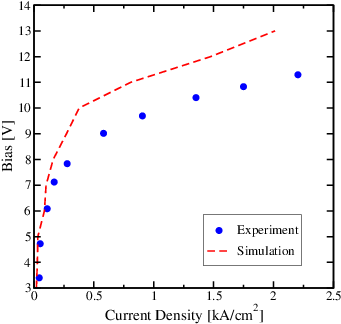
As in the simulations described before, we use a constant time step of 5 fs and monitor 10000 particles during 10 ps. According to the Monte Carlo algorithm presented in this work, we calculated the current density for this device and compared the obtained voltage-current characteristics with the measured values, which is illustrated in Figure 6.24. Electron scattering by polar optical and acoustic phonons, optical deformation potential interaction, inter-valley phonons, and interface roughness are included. The dashed curve displays the calculated current density for several bias points, while the symbols represent the measured values. The calculated and measured voltage-current characteristics are in good agreement, and the existing deviations can be attributed to the non-optimized scattering parameters and to additional scattering mechanisms not considered in the simulation.
Figure 6.25 shows the current density as a function of the temperature with and without interface roughness scattering. We observe a weak dependence of the current density on temperature, which can be explained by the dominance of electron scattering due to PO-phonon emission.
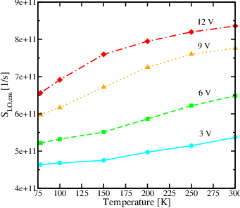
The scattering rate due to emission of polar optical phonons as a function of temperature for different bias points is plotted in Figure 6.26. A weak temperature dependence can be seen from this diagram.
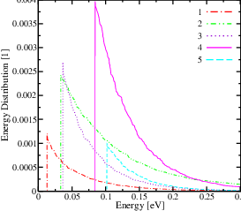
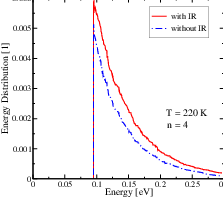
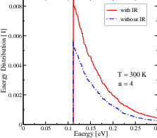
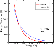
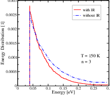
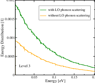
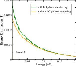
The dominance of electron scattering due to polar optical phonons is clearly illustrated by Figure 6.27 where the energy distributions of the upper and lower laser levels are depicted. The orange curves show the results without polar optical phonon scattering and the green ones illustrate the results including scattering due to polar optical phonons. We observe an increase in the occupation of the upper level and the lower level, while the increase of the upper level is much more significant compared to the lower level. The results plotted in this Figure fully support the notion that the polar optical phonon scattering mechanism is essential in order to provide a good condition for population inversion.
Since one of the aims in designing QCL structures is to obtain a significant population inversion between the upper and lower laser level, it is crucial to find out what mechanisms are decisive to achieve it. Our modeling approach was able to demonstrate that the scattering due to polar optical phonons is mainly accounting for this behavior regarding this MIR QCL design.
The comparison between the calculated and the measured current density suggests that there are also other important mechanisms which should be considered in order to get more realistic results.
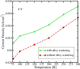
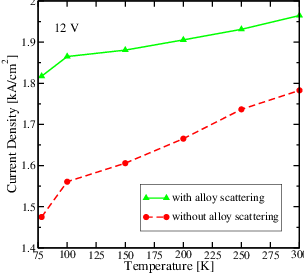
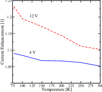
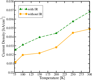
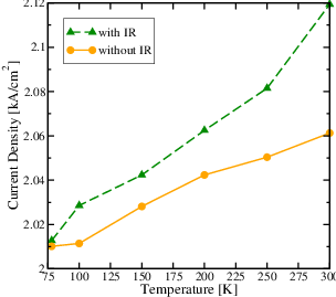
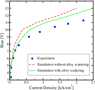
Figure 6.28 shows the calculated voltage-current characteristics when the alloy scattering is included in the simulation which is performed at 78 K. Due to its significant effect on the simulation results, the comparison with the experimental measurements gets sensitively better. In the following, we will investigate the impact of alloy scattering for higher temperatures. Table 6.5 shows the temperature dependence of the band gap energies of In0.53Ga0.47As and GaAs0.51Sb0.49 as well as the conduction band discontinuity [4]. Figure 6.29 illustrates the effect of the alloy scattering mechanism in dependence on the temperature. This scattering mechanism is mostly dominant at low temperatures, and somewhat weaker at high temperatures. This circumstance is also depicted in Figure 6.30. The ratio of the calculated current densities with and without taking into account alloy scattering is shown. We conclude that the alloy scattering mechanism is necessary to be considered in transport modeling of QCLs, especially in the low temperature region.
| T [K] | Eg(In0.53Ga0.47As) [eV] | Eg(GaAs0.51Sb0.49) [eV] | ΔEc [eV] |
| 78 | 0.7756 | 0.7869 | 0.1613 |
| 100 | 0.7723 | 0.7820 | 0.1597 |
| 150 | 0.7649 | 0.7739 | 0.1590 |
| 200 | 0.7507 | 0.7590 | 0.1583 |
| 250 | 0.7360 | 0.7412 | 0.1552 |
| 300 | 0.7209 | 0.7237 | 0.1528 |