


Next: 2.5 Fabrication
Up: 2. The Processing Chain
Previous: 2.3 Layout
Subsections
2.4 Mask Generation
A fundamental requirement for almost all useful semiconductor devices is the
definition of patterned elements. The main stream technology choice for
patterning has been optical lithography. Up to the early 70's lithography was
done as a contact printing process in which blue or near UV
light was passed through a photo mask directly onto a photo resist coated
semiconductor substrate [30].This shadow imaging process has been
described in many research publications and
handbooks [31], [32].
Beginning in the early 80's a new class of projection exposure tools, known as
steppers, was introduced [33]. For the first time the pattern
definition imaging on the semiconductor wafers was performed one chip at a
time in a step-and-repeat fashion. Most stepper systems employed a reduction
projection lens to ease the fabrication difficulty of the photo mask and to
improve the overall precision and accuracy of the overlay of patterns on the wafer.
Even more recently a combination of the earlier scanning approach with the
step-and-repeat approach was created [34]. The step-and-scan approach has spread
rapidly throughout the lithography tool industry, and is used for critical
layers (like gate, metallization and contact layers) at the 250nm node and
below [35].
Until the mid 90's all optical photo masks have been chrome on glass (called
COG-photo masks) [36], also called binary photo masks. Starting from the 350nm node
significant innovations in binary masks such as OPC (optical proximity correction) [37] and
AAPSM (alternating aperture phase shift masks) [38] were introduced which improved
the resolution capability of binary photo masks. A second approach besides the
binary photo masks then emerged as EAPSM (embedded attenuated phase shift
masks) [39] also called HTM (half tone masks).
Lithography is based on replicating the pattern on a photo mask into
resist covered wafers. In an ideal case without degradation in the
imaging process, a simple copy of the mask pattern would result, as shown in
Figure 2.4 a.
Figure 2.4:
Basic imaging
characteristics (a) Ideal shadow imaging; (b) Diffraction-broadened
projection imaging
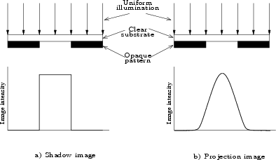 |
However, in a projection process the imaging is always subject to
degradation from diffraction and from imperfections in the projection
system. An example of the image from a diffraction-limited projection system
is shown in Figure 2.4 b.
The spreading of the image profile results from the wave nature of light, and
it is this property that limits the resolution capability of
optical imaging systems. In an imaging lens system with a circular aperture of
radius
 and imaging distance
  , the image intensity resulting from a point
source can be described by an expression containing a first order
BESSEL function,
, the image intensity resulting from a point
source can be described by an expression containing a first order
BESSEL function,
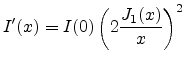 |
(2.1) |
where
 and
and  is the distance in
the image plane from the geometrical image point.
is the distance in
the image plane from the geometrical image point.  is the wavelength
of the monochromatic light source. A detailed deduction of this
expression is given in Appendix E.2. The fraction
is the wavelength
of the monochromatic light source. A detailed deduction of this
expression is given in Appendix E.2. The fraction
 given by
 for for |
(2.2) |
equals the numerical aperture  defined by
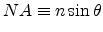 |
(2.3) |
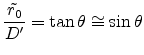
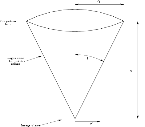
with n as the refractive index of the medium behind the aperture or lens.
Therefore the expression for  can be further simplified to
 .
For air as medium (
.
For air as medium (
 ) a simplified description of is given in
Figure 2.5 as
) a simplified description of is given in
Figure 2.5 as

Figure 2.5:
Geometric
situation in simple projection optical system
 |
This light intensity distribution is known as the AIRY pattern, after
G.B. AIRY who first derived it in 1835 [40]. In addition to the
general shape of the curve, shown in Figure 2.6, the first zero value
is of interest. At about
 occurs a intensity minimum and an
intensity maximum at
occurs a intensity minimum and an
intensity maximum at
 .
.
Figure 2.6:
Light
intensity distribution from a point source projected through a circular
imaging lens. The variable x on the horizontal axis is defined in the text
|
|
Resolution is defined as the ability to distinguish components of an
object or a group of objects. The resolution capability of astronomical
telescopes was studied in detail by LORD RAYLEIGH in the 19th
century [41]. He defined the limit of resolution for a telescope
as the angular separation between two stars when the peak of the
AIRY intensity pattern from one star coincided with the first
minimum of the AIRY intensity pattern for the other star.
This leads to the well-known RAYLEIGH condition for angular
resolution
 |
(2.4) |
where
is again the radius of the imaging objective aperture.
A sketch of the RAYLEIGH resolution condition is shown in
Figure 2.7. Note that the intensity at the midpoint between
the image peaks is reduced to about 78% of the peak intensity, which provides
discernible separation, but not with high contrast between the bright and dark
regions.
Figure 2.7:
RAYLEIGH criterion for resolution of two point images in (a)
1D and (b) 2D. Scale is the same as in Figure 2.6
|
|
While the analogy of astronomical imaging to photo lithography is not
completely quantitative, some key observations can be made. There is a limit
to resolution for any given optical projection system, and it is not possible
to resolve arbitrarily small or closely spaced features. It is also apparent
that the resolution can be improved by using a smaller wavelength of the
exposure light, and the resolution can be improved by making the projection
system aperture larger.
In practical lithography the RAYLEIGH condition is typically restructured into
the ``RAYLEIGH equation''
 |
(2.5) |
where  is the numerical aperture of the projection system and
  is a
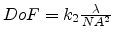
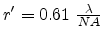
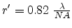
constant in the order of 0.4-0.8. There is no rigorous optical definition for
the constant , and it is generally used as a qualitative descriptor of
the overall lithography process capability. More details on the RAYLEIGH
equation are given in Table 2.1. Table 2.2
shows the numeric aperture, the resolution, and the depth of focus for the
most important wavelengths in lithography.
is a
constant in the order of 0.4-0.8. There is no rigorous optical definition for
the constant , and it is generally used as a qualitative descriptor of
the overall lithography process capability. More details on the RAYLEIGH
equation are given in Table 2.1. Table 2.2
shows the numeric aperture, the resolution, and the depth of focus for the
most important wavelengths in lithography.
Table 2.1:
Definitions for important
wavelength nodes in lithography
| Definitions |
|
|---|
| (g-line) |
436 nm |
| (i-line) |
365 nm |
| (KrF) |
248 nm |
| (ArF) |
193 nm |
( ) ) |
157 nm |
| Resolution |
|
|---|
| RAYLEIGH Resolution |
 |
| Traditional |
 |
| Advanced |
 |
| Depth of Focus |
|
|---|
| RAYLEIGH Depth of Focus |
 |
| Traditional |
 |
|
This common description of resolution capability is closely related to the
AIRY pattern described above. In particular, the first minimum of
the AIRY pattern occurs at about
 , and the
first maximum occurs at
, and the
first maximum occurs at
 . The qualitative agreement
with the usual range of is apparent.
. The qualitative agreement
with the usual range of is apparent.
High performance optical projection imaging for lithography is strongly
impacted by diffraction effects as noted in several previous sections. One
result of this behavior is that individual pattern features do not image
independently, but rather they interact with neighboring pattern features. A
detailed analysis of the projection imaging process, for example, the analysis
described in the paper by Hopkins [42], considers contributions
from every portion of the reticle object and every portion of the projection
optics in determining the exact image at the wafer plane. A simple heuristic
argument considers the extended diffraction structure of the AIRY
function comprising of the additional local maxima in the intensity
distribution. Overlap of the diffraction peaks with adjacent pattern features
leads to increased or decreased exposure intensity at any point in the image,
compared to a purely geometrical image model.
Next: 2.5 Fabrication
Up: 2. The Processing Chain
Previous: 2.3 Layout
R. Minixhofer: Integrating Technology Simulation
into the Semiconductor Manufacturing Environment
![\includegraphics[origin=cc,height=0.8\textwidth,clip=true]{figures/airy_pattern.rot.ps}](img62.png)
![\includegraphics[origin=c,width=7.2cm,clip=true]{figures/rayleigh_criterion_1d.rot.ps}](img64.png)
![\includegraphics[height=6cm,clip=true]{figures/rayleigh_criterion_2d.ps}](img65.png)