


Next: 3.8 Electrical Key-Parameter Extraction
Up: 3. The TCAD Concept
Previous: 3.6 Contact Definition
Finally, the data structure is ready for processing with device simulation. The
main inputs for device simulation are:
- Doping concentration of different doping species (e.g. Arsen,
Phosphorus, Antimony, Boron etc.) on a mesh.
- Structural information about the shape of the region which has to be
evaluated with device simulation. This information includes material types
of layers, topological variation of layers and the detailed surface and
interface shapes of the materials present in the structure.
- Named contacts as source for adjustable boundary conditions of the
device simulation.
An example for a typical input structure for device simulation is shown in
Figure 3.12. The three main input classes (doping,
structural and contact information) can be clearly seen.
Figure 3.12:
Example for a typical input structure for device simulation
comprising of doping concentration (a) including the different doping
species e.g. Boron (b) on a mesh and the topological structure and contact definition (d).
|
|
The semiconductor device simulators are fairly similar in their solution
approach. They all solve a system of partial
differential equations describing the potential distribution and carrier
transport in a doped semiconducting material.
The standard semi-classical transport theory is based on the BOLTZMANN equation [131],[132]
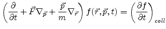 |
(3.1) |
where  is the position,
  is the impulse,
  is the electric field vector and
 is the
distribution function. In the simplest approach for solving this
equation the collision term on the right hand side of
(3.1) is substituted with a phenomenological
term
is the
distribution function. In the simplest approach for solving this
equation the collision term on the right hand side of
(3.1) is substituted with a phenomenological
term
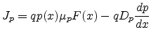
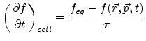 |
(3.2) |
where  indicates the (local) equilibrium distribution
function, and
indicates the (local) equilibrium distribution
function, and  is a microscopic relaxation time. It is very
useful to express the distribution function in terms of velocity,
rather than impulse, since it will be easier to calculate electrical
currents. In equilibrium one may use the MAXWELL-BOLTZMANN distribution function
is a microscopic relaxation time. It is very
useful to express the distribution function in terms of velocity,
rather than impulse, since it will be easier to calculate electrical
currents. In equilibrium one may use the MAXWELL-BOLTZMANN distribution function
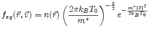 |
(3.3) |
where
 is the carrier density,
  is the lattice
temperature and
is the lattice
temperature and  is the effective mass. The use of
(3.3) for semiconductors is
justified in equilibrium as long as degeneracy is not present. the
carrier density
is directly related to the distribution
function according to
is the effective mass. The use of
(3.3) for semiconductors is
justified in equilibrium as long as degeneracy is not present. the
carrier density
is directly related to the distribution
function according to
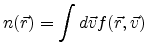 |
(3.4) |
which is of general applicability. The significance of the momentum
relaxation time can be understood if the electric field is switched
off instantaneously and a space-independent distribution is
considered. The resulting BOLTZMANN equation is then
 |
(3.5) |
which shows that the ralaxation time is a characteristic decay
constant for the return to the equilibrium state.
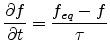
The often used drift-diffusion current equations
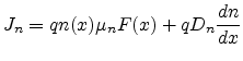 |
|
 |
(3.6) |
can be easily derived directly from the BOLTZMANN equation as outlined in
Appendix D. All device simulators use the
drift-diffusion approach as the simplest model to cover the transport effects
inside the semiconductor material.
Next: 3.8 Electrical Key-Parameter Extraction
Up: 3. The TCAD Concept
Previous: 3.6 Contact Definition
R. Minixhofer: Integrating Technology Simulation
into the Semiconductor Manufacturing Environment
![\includegraphics[origin=c,width=0.95\textwidth,clip=true]{figures/Sige_doping.rot.ps}](img154.png)
![\includegraphics[origin=c,width=0.95\textwidth,clip=true]{figures/Sige_boron.rot.ps}](img155.png)
![\includegraphics[origin=c,width=0.95\textwidth,clip=true]{figures/Sige_mesh.rot.ps}](img156.png)
![\includegraphics[angle=0,origin=c,width=0.85\textwidth,clip=true]{figures/Sige_boundary.rot.ps}](img157.png)