6.1 Transfer of Semiconductor Diffusion and Oxidation Process Recipes
Between 4" and 8" Wafer Fabrication Facilities
TCAD has found to be very useful in reducing the risks of semiconductor
process flow transfer between different fabrication facilities [154].
When transferring diffusion or oxidation process recipes from one type of
equipment (e.g. 4" diffusion furnace) to another type of equipment (e.g. 8"
diffusion furnace), it is generally not possible to copy the diffusion recipe
without modifications.
Especially, the temperature ramp rates for 8" diffusion recipes are usually
significantly slower than for 4" equipment. The main reason for this difference is
the different mechanical stability of 8'' and 4'' wafers. A plastic
deformation of the 8'' wafers called
``Furnace Slip'' is occurring during high temperature processing, if the
temperature ramp rates are too steep [155]. A table of maximum
allowable temperature ramp rates for a vertical 8'' furnace is given in
Table 6.1.
Table 6.1:Maximum allowable temperature ramp rates for vertical 8'' furnaces
Temperature
Ramp-Up
Temperature
Ramp-Down
Range
Rate
Range
Rate
-
/min
-
/min
-
/min
-
/min
-
/min
-
/min
-
/min
-
/min
Although, because of this constraint, the recipes might differ
significantly, the impact on the wafer has to be nearly identical for 4" and 8"
equipment. Thus optimization of the diffusion recipes is needed in order to
make the differences in dopant distribution and oxide thickness between 4" and
8" recipes as small as possible.
The following procedure was followed to optimize the 8'' recipes:
The original 4'' recipe is changed according to the new maximum ramp rates
allowed.
The main step contributing mainly to the overall thermal budget is
identified.
A score function giving a minimization target for the optimization was
defined.
The length of the main program step in the process simulation was varied in an optimization loop
until the score function was minimized.
This algorithm was described already in
Section 3.4, Figure 3.7.
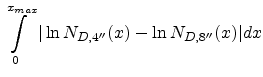
For optimization the framework SIESTA [144] was used. As a score
function
(6.1)
was chosen. is the depth measured from the surface into the wafer,
is the maximum depth of the process simulation region.
is the
resulting doping profile from the process simulation of the 4''
recipe.
is the resulting doping profile from the process
simulation of the 8'' recipe.
In Figure 6.1 the initial and final 8''
doping profile of a typical well diffusion recipe are shown.
Figure 6.1:Doping profile for a 4"
diffusion furnace compared to a 8" diffusion furnace before and after
optimization
The resulting 8'' diffusion recipe is shown in
Figure 6.2 in comparison to the 4''
recipe. The reduced temperature ramp rates of the 8'' recipe can be seen clearly.
Figure 6.2:Graphical comparison
between the 4" and 8" diffusion recipe for a typical p-well diffusion
For optimization of doping profiles with junctions (e.g. to the substrate) a
different score function, the well depth
may be used. As an
example a typical n-well diffusion program in a p-type substrate wafer is
shown in Figure 6.3
Figure 6.3:Graphical comparison between the 4" and 8" diffusion recipe for a typical n-well diffusion
The resulting junction depths versus diffusion time are
shown in Figure 6.4.
Figure 6.4:N-well junction depth over time of annealing step
Since the dependence of the junction depth on the diffusion time was exactly
linear in this case, by fitting a linear equation through the simulated points and extracting the
resulting annealing time, the 8'' program can be optimized without any
optimization loop like in the previous example.
![\includegraphics[origin=c,width=1.0\textwidth,clip=true]{figures/4inch_8inch_dopant_profile.rot.ps}](img210.png)
![\includegraphics[origin=c,width=1.0\textwidth,clip=true]{figures/4inch_8inch_thermal_profile.rot.ps}](img211.png)
![\includegraphics[origin=cc,width=1.0\textwidth,clip=true]{figures/E2A787_11787.rot.ps}](img213.png)
![\includegraphics[origin=cc,width=1.0\textwidth,clip=true]{figures/LOC17800_Optimization_Data.rot.ps}](img214.png)