Based on the principles shown in Section 2.4 some examples for proximity correction of masks and possible applications are given in the following sections.
The proximity correction of masks may be of importance, if structure sizes
approach the wavelength of the lithography system. At the 350nm node this is
the case for the ``Gate'' mask, the ``Active Area'' mask, the ``Contact'' mask
and the ``Metal 1'' mask. However in normal TCAD applications the proximity
effects of these masks are not taken into account, because the typical critical
dimensions of the front end masks (``Active Area'' and ``Gate'' which are have the
main impact on the device characteristics) are well controlled and are well
calibrated in the TCAD simulations. The back end masks are only interesting
for generating the contacts on top of the device. The detailed interconnect
shape is not of interest for routinely TCAD simulations. However, in the
application area of RF and high voltage, the exact interconnect shape is
influencing the analysis strongly in certain aspects. The equivalent RLC
network of the digital interconnect may impact the overall switching speed
strongly (at least at ground rules below 180nm) [156],[157],[158]. For high voltage ultra low
ohmic driver arrays with on-resistances in the milliohm range, the
metalization resistance is contributing more than 50% to the total
on-resistance.
These examples show, that an exact shape of the interconnect wires may impact
the overall simulation result quite strongly.
To obtain structures to analyze these influences more thoroughly with
simulation, first a proximity corrected layout has to be generated. The
detailed physics behind the generation of the corrected layout was described
already in Chapter 2. For the following examples
a modified version of LAYGRID [159],[160], the structure
generator for the finite element electro-thermal simulation tool
SAP [161],[162],[163] was used. The modification included
the implementation of the aerial image simulator LISI developed by Heinrich
Kirchauer [44] into the LAYGRID
software. The original (mask biased) CIF file was taken together with the
parameters of the lithography system (aperture etc.) as outlined
in [164] and [165] and submitted to the modified LAYGRID
code. The implemented LISI code generated a contour of every layer in the CIF
file comprising of the light intensities at the surface of the photo resist
(the aerial image). To obtain a fast and efficient simulation methodology the
complicated and time consuming calculation of the exact photo resist shape
after exposure and development was neglected. A certain threshold of the
illumination intensity of the aerial image was chosen and the iso-contours of
this intensity were extracted from the aerial image. This threshold was chosen
to match the width of the final CDs of isolated mask lines accordingly. The
contours were then written back into CIF file for further processing. The
resulting CIF format can be used by any commercial or university TCAD
simulator for further processing (e.g. process simulation). Examples for two
digital cells (an inverter and a bigger digital cell comprising of 22 CMOS
transistors) are shown in Figure 6.6 and Figure 6.7.
![$\textstyle \parbox{0.20\textwidth}{
\includegraphics[width=0.20\textwidth]{figures/inverter_layout.ps}\\
\centering (a)}$](img219.png)
![$\textstyle \parbox{0.20\textwidth}{
\includegraphics[width=0.20\textwidth]{figures/inverter_AA.ps}\\
\centering (b)}$](img220.png)
![$\textstyle \parbox{0.20\textwidth}{
\includegraphics[width=0.20\textwidth]{figures/inverter_P1.ps}\\
\centering (c)}$](img221.png)
![$\textstyle \parbox{0.20\textwidth}{
\includegraphics[width=0.20\textwidth]{figures/inverter_CO.ps}\\
\centering (d)}$](img222.png)
![$\textstyle \parbox{0.20\textwidth}{
\includegraphics[width=0.20\textwidth]{figures/inverter_M1.ps}\\
\centering (e)}$](img223.png)
![$\textstyle \parbox{0.20\textwidth}{
\includegraphics[width=0.20\textwidth]{figures/inverter_M1.ps}\\
\centering (f)}$](img224.png)
|
![$\textstyle \parbox{0.3\textwidth}{
\includegraphics[width=0.3\textwidth]{figures/big_cell_layout.ps}\\
\centering (a)}$](img225.png)
![$\textstyle \parbox{0.3\textwidth}{
\includegraphics[width=0.3\textwidth]{figures/big_cell_AA.ps}\\
\centering (b)}$](img226.png)
![$\textstyle \parbox{0.3\textwidth}{
\includegraphics[width=0.3\textwidth]{figures/big_cell_P1.ps}\\
\centering (c)}$](img227.png)
![$\textstyle \parbox{0.3\textwidth}{
\includegraphics[width=0.3\textwidth]{figures/big_cell_CO.ps}\\
\centering (d)}$](img228.png)
![$\textstyle \parbox{0.3\textwidth}{
\includegraphics[width=0.3\textwidth]{figures/big_cell_M1.ps}\\
\centering (e)}$](img229.png)
![$\textstyle \parbox{0.3\textwidth}{
\includegraphics[width=0.3\textwidth]{figures/big_cell_contours.ps}\\
\centering (f)}$](img230.png)
|
The resulting mask information was used to generate a three dimensional representation of the interconnect structures of the big digital cell with LAYGRID. A comparison of the metalization, and gate lines with and without proximity correction is given in Figure 6.8.
|
This structure can be used for further analysis of capacitance coupling, extraction of the RLC components of the interconnect or the overall metalization resistance.
Non-volatile memories (NVM) [166],[167],[168] play an important role in modern System-on-a-Chip (SoC)
solutions. The increasing demand of user-programmable information in such
systems has led to
new challenges in designing circuits with a certain amount of memory. NVMs are
typically used in mobile, small systems for flexible applications which
require variable information storage.
A variety of NVMs is available, each having different
specifications according to the structure of the selected cell. A
comprehensive overview is given in [169]. Two different programming
principles can be identified, hot-electron injection (HEI) [170] and
FOWLER-NORDHEIM (FN) tunneling [171],[172]. This work concentrates on an architecture that
uses FN tunneling as the programming mechanism. This EEPROM cell was
developed by J.M. Caywood [173],[174] and combines good endurance and reliability with a
simple structure and good performance with average area consumption.
The EEPROM p-channel memory cell was implemented in a common
0.35![]() CMOS process flow. The front-end-process flow is presented in
Figure 6.9. The detailed schematics for the EEPROM process module steps may be
found elsewhere [174].
CMOS process flow. The front-end-process flow is presented in
Figure 6.9. The detailed schematics for the EEPROM process module steps may be
found elsewhere [174].
|
Several implications arise for integrating an EEPROM memory in a CMOS
process.
First, the programming and erasing operation requires voltages up to 15V, which
are normally far above the breakdown voltage of the S/D junctions (this is the
case for technology nodes below 0.6![]() and gets more severe for
state-of-the-art nodes e.g. 130nm and beyond). Second, the added complexity of
the overall process flow must not increase to a level where dual-chip packaging
are cheaper solutions. As a consequence a maximum of only 2-4 additional mask
alignments are acceptable. Third, the thermal budget of the high-voltage gate
oxide for the control-gates will disturb sensitive threshold adjust implants
and must therefore be placed before them. Fourth, for EEPROM memory operations
additional high voltage devices are necessary to enable the generation of the
programming voltage via charge pumps and to switch these voltages for the cell
programming and erasing.
As a consequence of these constraints the EEPROM-module must be integrated after
the steps with the high thermal budget (e.g. the well diffusions)
and before the sensitive threshold adjust and LDD steps which determine the
standard CMOS logic. Since the base CMOS process offers already a dual gate (3.3V
and 5V) analog mixed-signal option, the integrated flow includes three gate
oxides. The HV-gate oxide of the cell is integrated right before the 3.3V
and 5V gate oxides (refer to Figure 6.9).
To get a deeper insight into the integration challenges, TCAD (Technology
Computer Aided Design) simulations were
used to find the best solution for the EEPROM module integration. Furthermore,
the cell characteristics were optimized and the prediction of the electrical
characteristics was used to generate preliminary SPICE models of the
cell. This enabled a very early start of the memory block design. Additionally
the transient behavior of the cell in programming operation was evaluated by TCAD.
and gets more severe for
state-of-the-art nodes e.g. 130nm and beyond). Second, the added complexity of
the overall process flow must not increase to a level where dual-chip packaging
are cheaper solutions. As a consequence a maximum of only 2-4 additional mask
alignments are acceptable. Third, the thermal budget of the high-voltage gate
oxide for the control-gates will disturb sensitive threshold adjust implants
and must therefore be placed before them. Fourth, for EEPROM memory operations
additional high voltage devices are necessary to enable the generation of the
programming voltage via charge pumps and to switch these voltages for the cell
programming and erasing.
As a consequence of these constraints the EEPROM-module must be integrated after
the steps with the high thermal budget (e.g. the well diffusions)
and before the sensitive threshold adjust and LDD steps which determine the
standard CMOS logic. Since the base CMOS process offers already a dual gate (3.3V
and 5V) analog mixed-signal option, the integrated flow includes three gate
oxides. The HV-gate oxide of the cell is integrated right before the 3.3V
and 5V gate oxides (refer to Figure 6.9).
To get a deeper insight into the integration challenges, TCAD (Technology
Computer Aided Design) simulations were
used to find the best solution for the EEPROM module integration. Furthermore,
the cell characteristics were optimized and the prediction of the electrical
characteristics was used to generate preliminary SPICE models of the
cell. This enabled a very early start of the memory block design. Additionally
the transient behavior of the cell in programming operation was evaluated by TCAD.
To predict the EEPROM cell behavior two main areas of operation had to be
investigated.
The accuracy of the DC characteristics of the cell is mainly determined by
the overall calibration of the TCAD environment. Since this calibration was
performed with the CMOS base process, the first results were already quite
accurate.
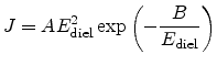
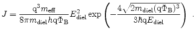
The transient programming characteristics however, showed significant
deviations from literature data [174]. The cause for these differences
were inaccurate FN-tunneling model parameters in the device simulator
DESSIS-ISE [83]. The most used model to describe tunneling is the FOWLER-NORDHEIM
equation [176]
 |
(6.2) |
The measurements were carried out on structured wafers with the tunnel oxide and a simple dot-masked polysilicon layer on top. The polysilicon dots were contacted with one needle of a micromanipulator, and the voltage between this contact and the wafer-chuck was varied appropriately.
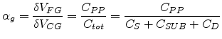
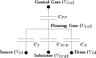
is the major contributor to cell speed. In order to optimize the cell speed, the
Control-Gate/Floating Gate Capacitance ![]() must be
maximized. Figure 6.12 shows all contributions to the coupling
ratio.
must be
maximized. Figure 6.12 shows all contributions to the coupling
ratio.
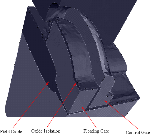
The coupling ratio of the EEPROM cell is already excellent, since the
special layout [174] enables an encapsulation of the floating-gate
by the control-gate on all sides. The main parameter left for increasing the
coupling-ratio is the thickness of the floating gate. However, there is a
tradeoff between floating gate thickness, step-coverage, and minimum cell
distance in a memory block.
Using three-dimensional TCAD-process- and device-simulations a parameter
optimum, matching the measurements, was found. Furthermore, the coupling-ratio of the
cell itself could be predicted. The process simulation was again calibrated by comparing the
three-dimensional TCAD boundary model with SEM pictures taken during
fabrication (Figure 6.13).
|
The final structure of the EEPROM cell obtained by three-dimensional process simulation, which serves as input for a finite element analysis [162] for the extraction of the capacitances and the coupling-ratio, is shown in Figure 6.14.
 |
The process simulation was performed by combining the simulation
tools DIOS-ISE [82] and TOPO3D [179] [180]. The formation of the
field oxide was carried out by a two-dimensional simulation performed with
DIOS-ISE. Due to the three-dimensional nature of the problem, switching to a full
three-dimensional analysis is required, beginning with the formation of the
floating gate. Therefore the two-dimensional structure generated by DIOS-ISE was expanded to a three-dimensional geometry representation. In the
following an isotropic deposition of the
poly-silicon layer was performed with TOPO3D which is a rigorous three-dimensional
simulator for etching and deposition processes. In order to transfer the
floating gate mask, an etching model of TOPO3D was applied,
which is capable of taking aerial image information into account. The aerial
image figure of the floating gate mask was produced by the aerial image
simulator LISI [181],[182],[183] and loaded into the topography simulator.
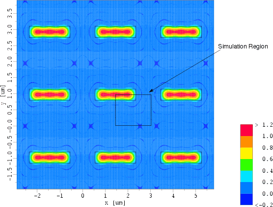
Worth mentioning is that the mask information for the aerial image simulation is
taken from a gds2-file containing a 3![]() 3 cell array to prevent
disturbances because of simulation domain boundaries (Figure 6.15).
3 cell array to prevent
disturbances because of simulation domain boundaries (Figure 6.15).
 |
|
TCAD methods are nowadays the method of choice for add-on module process integration. It was demonstrated that predictions for some technology key performance indicators can be derived. This methodology is excellently suited for a successful, timely and cost effective implementation of non-standard modules into a base process flow. In special cases three-dimensional process simulation is already feasible for industrial use.
This example deals with the coupled process and device simulation of a
laterally diffused PIN-diode of special shape and subsequent comparison of the
device simulation results to electrical measurements. Furthermore, it gives an
outlook to layout optimization of laterally diffused devices in general.
This example is one of the first fully integrated process and device
simulations including non-Manhattan type structures and full incorporation of
lithography proximity effects on photo resist level. Previous work was
constrained to Manhattan type (
![]() angles between boundary primitives)
structures without taking into account rigorous lithography simulation.
By applying this new methodology significant differences in electrical
characteristics between two-dimensional and three-dimensional simulations have
been obtained. The simulated device was a Zener-diode in a
angles between boundary primitives)
structures without taking into account rigorous lithography simulation.
By applying this new methodology significant differences in electrical
characteristics between two-dimensional and three-dimensional simulations have
been obtained. The simulated device was a Zener-diode in a ![]() CMOS technology process. This relatively "big" technology process was chosen to
demonstrate the impact of three-dimensional effects in device characteristics
even in such "old" process technologies. The layout of the element is of
inherent two-dimensional nature because of the
CMOS technology process. This relatively "big" technology process was chosen to
demonstrate the impact of three-dimensional effects in device characteristics
even in such "old" process technologies. The layout of the element is of
inherent two-dimensional nature because of the
![]() angles in the p+ and
n+ doped regions of the device. A complete process flow was simulated (see
Figure 6.16) including the following critical steps:
angles in the p+ and
n+ doped regions of the device. A complete process flow was simulated (see
Figure 6.16) including the following critical steps:
|
![\includegraphics[angle=0,origin=c,width=1.0\textwidth,clip=true]{figures/zener_convert.ps}](img260.png)
|
|
|
|
![\includegraphics[origin=c,width=1.0\textwidth,clip=true]{figures/zener_characteristics.rot.ps}](img266.png)
|
|
|
![\includegraphics[angle=0,origin=c,width=0.95\textwidth,clip=true]{figures/big_cell_prox.ps}](img231.png)
![\includegraphics[angle=0,origin=c,width=0.95\textwidth,clip=true]{figures/big_cell.ps}](img232.png)
![\includegraphics[width=0.8\textwidth]{figures/eeprom_process_flow.ps}](img233.png)
![\includegraphics[origin=c,width=0.7\textwidth,clip=true]{figures/Full_ONO_Cell.rot.ps}](img235.png)
![\includegraphics[origin=c,width=0.7\textwidth,clip=true]{figures/Spacer_ONO_Cell.rot.ps}](img236.png)
![\includegraphics[origin=c,width=0.7\textwidth,clip=true]{figures/Full_Oxide_Cell.rot.ps}](img237.png)
![\includegraphics[origin=c,width=1.2\textwidth,clip=true]{figures/Tunneling.rot.ps}](img240.png)
![\includegraphics[angle=0,origin=c,width=1.0\textwidth,clip=true]{figures/FG_last.ps}](img244.png)
![\includegraphics[angle=0,origin=c,width=0.8\textwidth,height=0.7\textwidth,clip=true]{figures/SEM_floating_gate.2.ps}](img245.png)
![\includegraphics[angle=0,origin=c,width=0.8\textwidth,clip=true]{figures/zener_process_flow.ps}](img259.png)
![\includegraphics[angle=0,origin=c,width=0.95\textwidth,clip=true]{figures/zener5675_bnd.ps}](img261.png)
![\includegraphics[angle=0,origin=c,width=0.95\textwidth,clip=true]{figures/zener6000_bnd.ps}](img262.png)
![\includegraphics[angle=0,origin=c,width=1.0\textwidth,clip=false]{figures/zener6000_msh.ps}](img263.png)
![\includegraphics[angle=0,origin=c,width=1.0\textwidth,clip=false]{figures/zener_device_bnd.ps}](img264.png)
![\includegraphics[angle=0,origin=c,width=1.0\textwidth,clip=false]{figures/zener_device_msh.ps}](img265.png)
![\includegraphics[angle=0,origin=c,width=0.95\textwidth,clip=true]{figures/zener_doping.ps}](img268.png)
![\includegraphics[origin=c,width=0.95\textwidth,clip=true]{figures/zener_junction_doping.rot.ps}](img269.png)
![\includegraphics[angle=0,origin=c,width=0.95\textwidth,clip=true]{figures/zener_potential.ps}](img270.png)
![\includegraphics[origin=c,width=0.95\textwidth,clip=true]{figures/zener_potential_contour.rot.ps}](img271.png)
![\includegraphics[angle=0,origin=c,width=0.95\textwidth,clip=true]{figures/zener_efield.ps}](img272.png)
![\includegraphics[angle=0,origin=c,width=0.95\textwidth,clip=true]{figures/zener_efield_contour.ps}](img273.png)
![\includegraphics[origin=c,width=0.95\textwidth,clip=true]{figures/zener_efield_250000_contour.rot.ps}](img274.png)
![\includegraphics[origin=c,width=0.95\textwidth,clip=true]{figures/zener_efield_600000_contour.rot.ps}](img275.png)