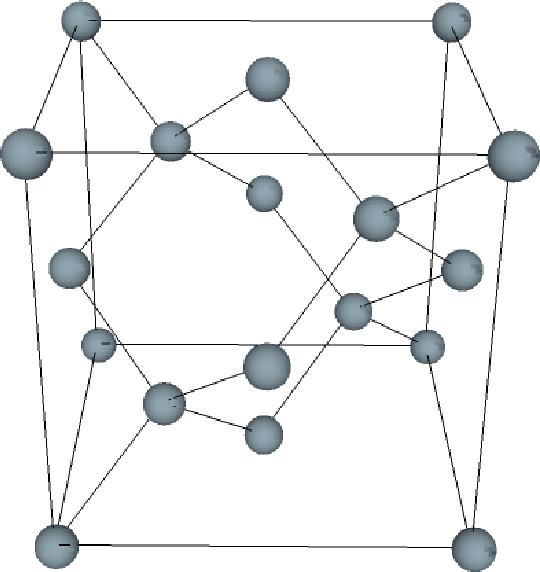
Figure 5.1: Sketch of the diamond crystal lattice.
In this chapter the effective k⋅p Hamiltonian with shear strain and properly included spin-orbit interaction is introduced. The wave functions and the valley splitting is investigated for different parameters.
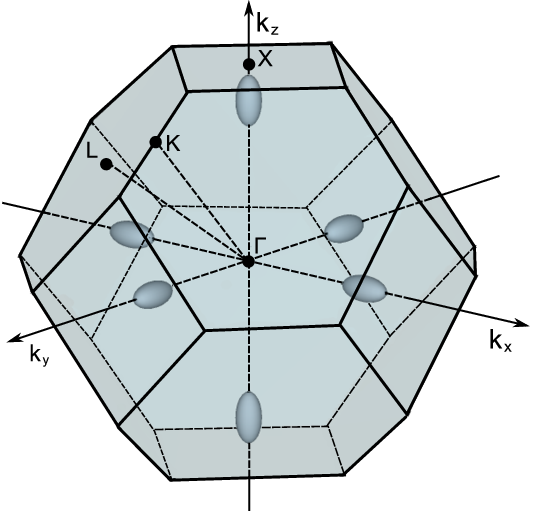
Silicon has a diamond lattice structure (Figure 5.1). The diamond lattice is of a face centered cubic Bravais lattice which contains two identical atoms per unit cell. The distance between the two atoms is equals to one quarter of the diagonal of the cube. The first Brillouin zone is sketched in Figure 5.2. It has the shape of a truncated octahedron and can be visualized with eight hexagonal faces and six square faces (Figure 5.2). The following symmetry points are shown: Γ the point in the center of the zone (origin of k space), X - the point in the middle of square faces, L - the point in the middle of hexagonal faces, and K - the point in the middle of the edge shared by two adjacent hexagons. The directions are: Δ - the axis connecting the Γ and X points, Λ - the axis connecting the Γ and L points, and Σ - the axis connecting the Γ and K points. The conduction band minima lie on the six equivalent Δ - lines and occur at about 85% of the way to the zone boundary.
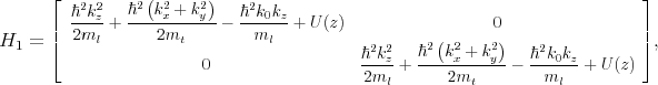
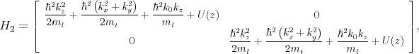
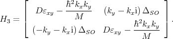
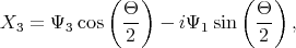
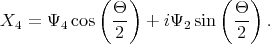
For [001] oriented valleys in a (001) silicon film the Hamiltonian is written in the vicinity of the X point along the kz-axis in the Brillouin zone. The basis is conveniently chosen as [(X1, ↑) , (X1, ↓) , (X2′, ↑) , (X2′, ↓)], where ↑ and ↓ indicate the spin projection at the quantization z-axis, X1 and X2′ are the basis functions corresponding to the two valleys. The effective k⋅p Hamiltonian reads as [111, 87, 106]
![[ H1 H3 ]
H = † ,
H 3 H2](disser84x.png) | (5.1) |
where H1, H2, and H3 are written as
 | (5.2) |
 | (5.3) |
 | (5.4) |
Here, εxy denotes the shear strain component, M-1 ≈ m t-1 - m 0-1, D=14eV is the shear strain deformation potential, mt and ml are the transversal and the longitudinal silicon effective masses, k0=0.15×2π∕a is the position of the valley minimum relative to the X point in unstrained silicon, and U(z) is the confinement potential.
The spin-orbit term τy ⊗ ΔSO(kxσx - kyσy) with [70]
![2 || ||
Δ = --ℏ--- |∑ ⟨X1-|pj|n-⟩⟨n-|[∇V--×-p-]j|X2′⟩|,
SO 2m30c2 || En - EX ||
n](disser88x.png) | (5.5) |
couples the states with the opposite spin projections from the opposite valleys. In the perturbation theory expression for ΔSO En is the energy of the n-th band at the X point, EX is the energy of the two lowest conduction bands X1 and X2′ degenerate at the X point, p is the momentum operator, V is the bulk crystal potential, σx, σy, and σz are the spin Pauli matrices, τy is the y-Pauli matrix in the valley degree of freedom and c is the speed of light.
In the presence of strain and confinement the four-fold degeneracy of the n-th unprimed subband is partly lifted by forming an n+ and n- subladder (the valley splitting), however, the degeneracy of the eigenstates with the opposite spin projections n±⇑⟩ and n±⇓⟩ within each subladder is preserved. |⇑⟩ is the superposition of the spin-up and the spin-down eigenstates, |⇓⟩ is the superposition of the spin-down and the spin-up eigenstates.
The degenerate states are chosen to satisfy
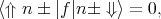 | (5.6) |
with the operator defined as [137]
 | (5.7) |
where θ is the polar φ and is the azimuth angle defining the orientation of the injected spin. In general, the expectation value of the operator f computed between the spin up and down states from different subladders is non-zero, when the effective magnetic field direction due to the spin-orbit interaction is different from the injected spin quantization axis
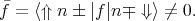 | (5.8) |
For a zero value of the confinement potential the energy dispersion of the lowest conduction bands is given by
 | (5.9) |
This expression generalizes the corresponding dispersion relation from [70] by including shear strain.
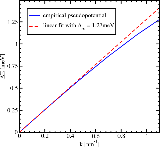
In order to evaluate the strength ΔSO of the effective spin-orbit interaction Equation 5.9 is used. Close to the X point in
the unstrained sample the gap between the X1 and X2′ conduction bands can be opened by ΔSO alone if one evaluates the
dispersion for kx≠0 but ky = kz = 0. The band splitting along the x-axis is then equal to the 2 . The empirical
pseudopotential method (EPM) [111], [117] is used to obtain the splitting numerically. The result is shown in Figure 5.3.
The dependence on kx is indeed linear at small values of kx. By fitting this dependence with a linear function
(shown in Figure 5.3) at small kx the value ΔSO = 1.27meVnm is found which is close to the one reported
in [70].
. The empirical
pseudopotential method (EPM) [111], [117] is used to obtain the splitting numerically. The result is shown in Figure 5.3.
The dependence on kx is indeed linear at small values of kx. By fitting this dependence with a linear function
(shown in Figure 5.3) at small kx the value ΔSO = 1.27meVnm is found which is close to the one reported
in [70].
To find the wave functions in a analytical manner, the Hamiltonian (5.1) is rotated by means of the following unitary
transformation. The four basis functions X1↑,X1↓,X2′↑,X2′↓ for the two [001] valleys with spin up, spin down are
transformed by (5.10-5.17) with tan  =
=  . The transformation decouples the spins with opposite direction
in different valleys.
. The transformation decouples the spins with opposite direction
in different valleys.
![[ ]
Ψ = 1- (X + X ′ ) + (X + X ′ )∘kx---iky-- ,
1 2 1↑ 2↑ 1↓ 2↓ k2x + k2y](disser97x.png) | (5.10) |
![[ ]
1 ( ) ( ) kx - iky
Ψ2 = -- X1 ↑ + X ′2↑ - X1 ↓ + X ′2↓ ∘--2----2- ,
2 kx + ky](disser98x.png) | (5.11) |
![[ ]
Ψ = 1- (X - X ′ ) + (X - X ′ )∘kx---iky-- ,
3 2 1↑ 2↑ 1↓ 2↓ k2x + k2y](disser99x.png) | (5.12) |
![[ ]
1 ( ′ ) ( ′ ) kx - iky
Ψ4 = -- X1 ↑ - X 2↑ - X1 ↓ - X 2↓ ∘--2----2- ,
2 kx + ky](disser100x.png) | (5.13) |
 | (5.14) |
 | (5.15) |
 | (5.16) |
 | (5.17) |
The Hamiltonian (5.1) can now be cast into a form in which spins with opposite orientation in different valleys are independent
![[ H H ]
H = 1 3 ,
H3 H2](disser105x.png) | (5.18) |
 1, 2, and 3 are written as
 | (5.19) |
 | (5.20) |
![[ ]
ℏ2k0kz 0
H3 = ml ℏ2k0kz
0 --ml-](disser108x.png) | (5.21) |
with δ = 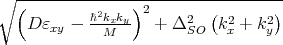 .
.
Following [111] the wave functions are found analytically in the same manner as for the two band k⋅p Hamiltonian written in the vicinity of the X-point of the Brillouin zone for silicon films under uniaxial strain.
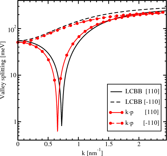
In order to validate the Hamiltonian the analytical results are compared to other approaches. For instance, Figure 5.4 shows the splitting between the lowest unprimed electron subbands as a function of the wave vector k taken along [110] and [-110] directions in a confined system. The results computed by the linear combination of bulk bands (LCBB) method [30] and the perturbative k⋅p approach are shown. For the [-110] direction the dependence is smooth without any sharp features. For the curves calculated along [110] direction a sharp decrease of the splitting is observed. Although the positions of the minima calculated by the k⋅p and by the LCBB methods do not match completely, the agreement is quite spectacular.
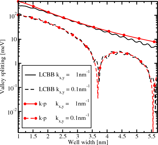
The valley splitting in a quantum well as a function of the well width is shown in Figure 5.5. The in-plane wave vector k along the [110] direction is chosen. The results for the wave vectors with the components kx=0.1nm-1, k y=0.1nm-1 and kx=1nm-1, k y=1nm-1 are shown for convenience. As predicted [38, 118], the valley splitting develops sharp minima for small values of k. For larger k the valley splitting computed with the k⋅p method decays monotonically when the film thickness is increased. The results obtained by the LCBB methods are in good agreement with those obtained by the k⋅p approach.
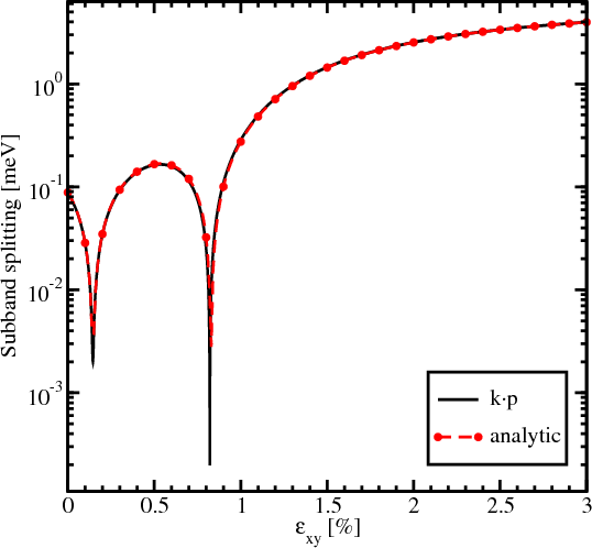
Finally, the analytical solution is compared to the numerical [7]. Figure 5.6 demonstrates an excellent agreement between the analytical and the numerically obtained results for a silicon film of 4nm thickness for kx=0.25nm-1 and ky=0.25nm-1. For the numerical calculations a barrier of 10eV height has been assumed.
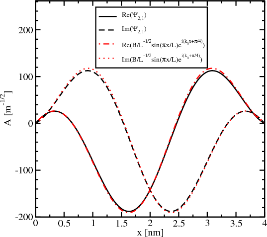
The eigenvector for the Hamiltonian (Equation 5.18) for the lowest subband is a four-component vector. For k = 0 spin-up and spin-down states are eigenstates, i.e. spin-up wave-function does not contain any spin-down states and vice versa. For kx≠0 or ky≠0 the spin-orbit term does not vanish, thus, two eigenstates are mixed. Therefore, the four-component wave function for spin-up electron contains a finite but small part of the spin-down state. Figure 5.7 shows the small spin-down component of the spin-up wave-function in a valley along [001] direction. The wave functions is quite accurately described by its envelope function times the phase factor eik0z+ϕ, where ϕ is the wave functions phase.
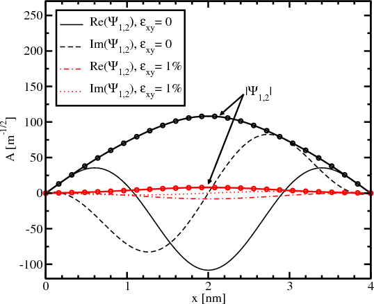
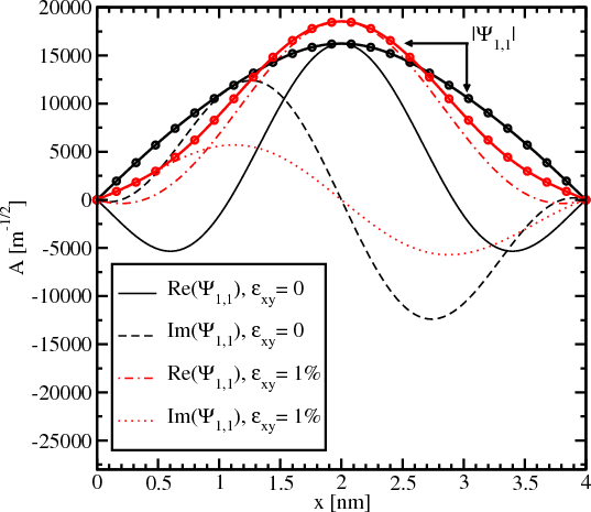
Figure 5.8 and Figure 5.9 show the majority and the minority components of the spin-up wave function for different shear strain values. The absolute value of the small part of the wave function shown in Figure 5.8 significantly decreases with strain applied. The derivative at the interface also becomes smaller for the strain value of 1% compared to the unstrained wave function. The absolute value of the big component of the wave function shown in Figure 5.9 changes insignificantly.
The decrease of the spin-down component in the spin-up wave function leads to a decrease of the Elliott contribution (Equation 4.50) to the spin relaxation.
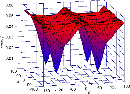
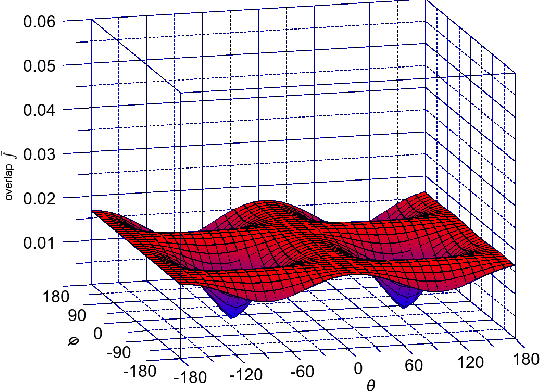
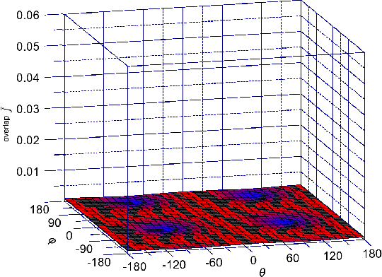
Figure 5.10, Figure 5.11, and Figure 5.12 show the dependence of (Equation 5.8) on the orientation of the injected spin for kx = 0.1nm-1, k y = 0.1nm-1 for different values of shear strain. The absolute value of the overlap characterizes the strength of the spin up/down states mixing caused by the spin-orbit interaction. The spin mixing significantly decreases with shear strain increased in the whole range of spin orientations.
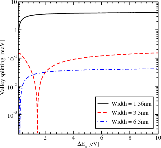
In this section the value of the energy splitting between the subbands with the same quantum number n but from different subsets n+ and n- as a function of the conduction band offset at the interface and for different values of the quantum well thickness is investigated. It is assumed that the spin is injected along the z-direction and the components of the wave vector k are kx=0.1nm-1 and k y=0.1nm-1. Figure 5.13 shows the subband splitting for three different values of the film width, namely 1.36nm, 3.3nm, and 6.5nm.
The Schr¨odinger differential equation, with the confinement potential appropriately added in the Hamiltonian (5.1), is solved using efficient numerical algorithms available through the Vienna Schr¨odinger-Poisson framework (VSP)[62, 7].
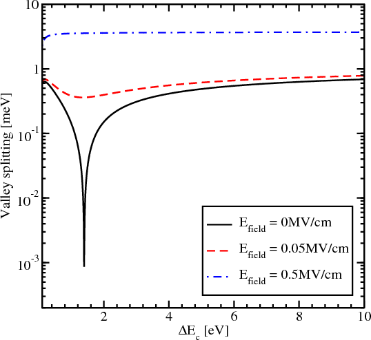
Figure 5.13 demonstrates a complicated behavior which strongly depends on the thickness value, in contrast to the valley splitting theory in SiGe/Si/SiGe quantum wells [38], which predicts that in the case of a symmetric square well without an electric field the valley splitting is simply inversely proportional to the conduction band offset ΔEC at the interfaces. Figure 5.13 shows that for the quantum well of 1.36nm width the splitting first increases but later saturates. For the quantum well of 3.3nm width a significant reduction of the valley splitting around the conduction band offset value 1.5eV is observed. A further increase of the conduction band offset leads to an increase of the subband splitting value. For the quantum well of 3.3nm thickness the valley splitting saturates at about 0.17meV.
For the quantum well of 6.5nm width a significant reduction of the valley splitting is observed around the conduction band offset value of 0.2eV. The subband splitting saturates at a value of 0.04meV. Although for the values of the conduction band offset smaller than 4eV the valley splitting depends on ΔEC, for larger values of the conduction band offset it saturates.
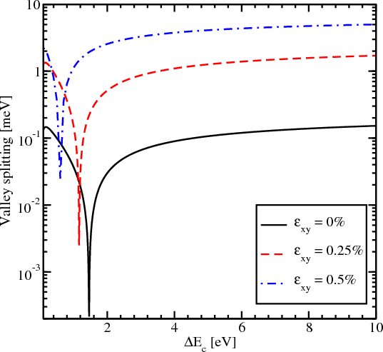
The valley splitting dependence on strain as a function of the conduction band offset for the film of 3.3nm thickness is shown in Figure 5.14. Without shear strain the valley splitting is significantly reduced around the conduction band offset value of 1.5eV. For the shear strain value of 0.25% and 0.5% the sharp reduction of the conduction subbands splitting shifts to a smaller value of ΔEC. However, the region of significant reduction is preserved even for the large shear strain value of 0.5%. The value of the valley splitting at saturation for large shear strain is considerably enhanced as compared to the unstrained case.
The influence of the effective electric field on the region of sharp splitting reduction is demonstrated in Figure 5.15. With the electric field applied the reduction in the region of interest around the conduction band offset value 1.5eV becomes smoother. However, for values of the conduction band offset smaller than 1.5eV the reduction of the valley splitting is still observed. For the values larger than 1.5eV the subband splitting slightly increases and then saturates. For the electric field value of 0.05MV/cm the saturation value of the valley splitting is almost equal to the saturated valley splitting value without electric field. For the stronger electric field of 0.5MV/cm the valley splitting reduction vanishes completely and the splitting becomes almost independent of the conduction band offset.
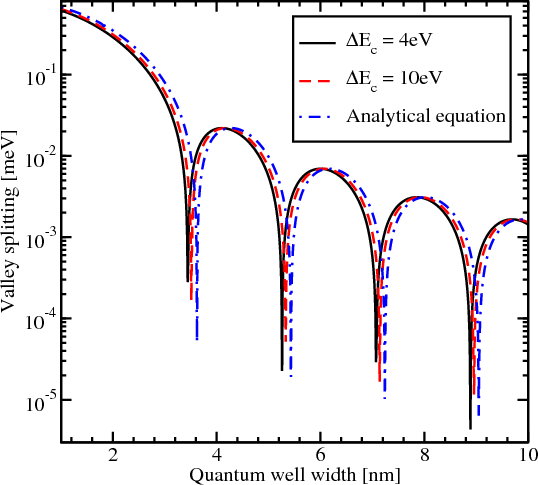
The splitting of the lowest unprimed electron subbands as a function of the silicon film thickness for several values of the conduction band offset at the interfaces is shown in Figure 5.16. The valley splitting oscillates with increasing film thickness. According to the theory [9], the equation for the valley splitting in an infinite potential square well is generalized including the spin-orbit coupling as [111, 124]
 | (5.22) |
with yn, η, and B defined as
 | (5.23) |
 | (5.24) |
 | (5.25) |
Here t is the film thickness. As it was shown earlier the conduction band value of 4eV provides a subband splitting value close to the saturated one. Because (5.22) is written for an infinite potential square well, a slight discrepancy is observed between the theoretical curve and the numerically computed curve calculated for the conduction band offset value 4eV in Figure 5.16. A large value of the conduction band offset demonstrates a better agreement between the theory and numerically obtained results.
Following (5.22), the results shown in Figure 5.13 can be understood as a consequence of vanishing of the
 term. Although the conduction band offset is not included explicitly in the equation for
the valley splitting, it can be taken into account through an effective film width of a finite potential well
as [38]
term. Although the conduction band offset is not included explicitly in the equation for
the valley splitting, it can be taken into account through an effective film width of a finite potential well
as [38]
 | (5.26) |
 | (5.27) |
where E is the subband energy. Thus, increasing the potential barrier height leads to a decrease of the effective film thickness, which then results in the energy splitting dependence shown in Figure 5.13.
The valley splitting reductions shown in Figure 5.14 are also the result of the oscillating sine term in (5.22). The small
increase of the shear strain leads to a decrease of the  term. This means that in order to obtain zeros of the sine
term for larger shear strain values the effective quantum well thickness must be larger. A decrease in the conduction band
offset leads precisely to such an increase of the effective thickness. Thus, the results shown in Figure 5.14 are in very good
agreement with theory.
term. This means that in order to obtain zeros of the sine
term for larger shear strain values the effective quantum well thickness must be larger. A decrease in the conduction band
offset leads precisely to such an increase of the effective thickness. Thus, the results shown in Figure 5.14 are in very good
agreement with theory.
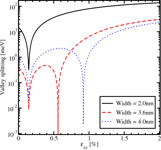
Figure 5.17 shows the dependence of the energy splitting on shear strain for the in-plane wave vector k components are
kx=0.25nm-1 and k
y=0.25nm-1. The significant valley splitting reduction around the strain value 0.145% appears to be
independent of the quantum well width. According to (5.22), the valley splitting is also proportional to B, and the valley
splitting reduction around the shear strain value 0.145% is caused by vanishing of the Dεxy - contribution. At this
minimum the valley splitting is determined by the spin-orbit interaction term alone. The other valley splitting minima
in Figure 5.17 depend on the film thickness and are caused by vanishing values of the
contribution. At this
minimum the valley splitting is determined by the spin-orbit interaction term alone. The other valley splitting minima
in Figure 5.17 depend on the film thickness and are caused by vanishing values of the  term.
term.
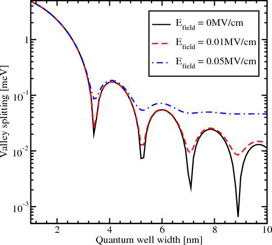
The valley splitting as a function of the quantum well width for different values of the effective electric field is shown in Figure 5.18. Without electric field the valley splitting oscillates as shown in Figure 5.16. With electric field the oscillations are not observed in thicker films. This is due to the fact that in thick films the subband quantization is caused by the electric field. Indeed, for thin structures, when the quantization is still caused by the second barrier of the quantum well, the shape of the oscillations is similar to that in the absence of an electric field. According to [38], the condition for the independence of the valley splitting from the quantum well width is
 | (5.28) |
For an electric field of 0.05MV/cm the quantum well width must be larger than 6.9nm in order to observe the valley splitting independent on the quantum well width. This value is in good agreement with the simulation results shown in Figure 5.18.
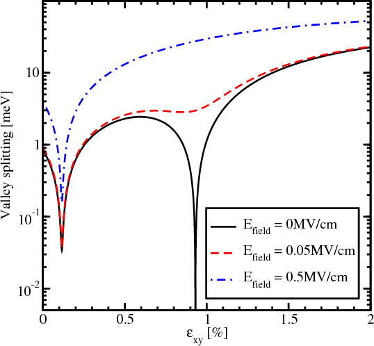
Figure 5.19 shows the dependence of the valley splitting on strain. Without electric field the valley splitting reduces significantly around the strain values 0.116% and 0.931% as shown in Figure 5.19. With electric field applied the minimum around the strain value 0.931% becomes smoother, however, for a strain value around 0.116% the sharp reduction of the valley splitting is preserved. For a large electric field the valley splitting reduction around the value 0.931% vanishes completely.
For the strain value 0.116% the sharp reduction of the valley splitting is still preserved at a minimum value only slightly
affected by the electric field. As follows from (5.22), for kx=0.5nm-1, k
y=0.1nm-1 the strain value 0.116% causes the term
Dεxy - to vanish and minimizes the valley splitting, in good agreement with the first sharp valley splitting reduction
in Figure 5.19. Thus, the valley splitting at this strain value is solely determined by the spin-orbit interaction term. The
second minimum in the valley splitting around the strain value 0.931% in Figure 5.19 is caused by vanishing of the
to vanish and minimizes the valley splitting, in good agreement with the first sharp valley splitting reduction
in Figure 5.19. Thus, the valley splitting at this strain value is solely determined by the spin-orbit interaction term. The
second minimum in the valley splitting around the strain value 0.931% in Figure 5.19 is caused by vanishing of the
 term. The effective electric field alters the confinement in the well and is therefore able to
completely wash out the minimum in valley splitting due to the sine term. However, in agreement with (5.22),
it can only slightly affect the first minimum due to the shear strain dependent contribution, in agreement
with Figure 5.19.
term. The effective electric field alters the confinement in the well and is therefore able to
completely wash out the minimum in valley splitting due to the sine term. However, in agreement with (5.22),
it can only slightly affect the first minimum due to the shear strain dependent contribution, in agreement
with Figure 5.19.