Since the invention of integrated circuits many advancements in processing technologies have
been achieved. Electronic devices are used daily and therefore they have enormously impacted
our lives and life without them would be unfathomable. Thus, the reliability issues connected to
newly developed devices are of great technical and economic interest.
Integrated circuits (ICs) are an integral component of electronic devices such as computers,
mobile phones, and other digital home appliances. ICs are simply very advanced electric circuits
consisting of active and passive components. The most frequently implemented passive
components are resistors and capacitors while the active components are diodes and transistors.
Each component has a specific task to perform and they all have to work together to
make the circuit perform as desired. Resistors are used to adjust signal levels, to
limit current flow, bias active elements, and terminate transmission lines. Capacitors
permit to temporarily store electrical energy in an electric field. Diodes allow current
flow in only one direction and transistors are used to amplify or switch electronic
signals and electrical power. These components are interconnected together by a single
or multilevel metalization on a piece of single crystal silicon (Si) [4]. ICs range in
complexity from simple logic modules to entire microcomputers, incorporating millions of
components.
The first semiconductor-based electronic devices were constructed in 1947 for applications in
medicine, military and other areas [4, 5, 6]. The first transistors were connected together with
traces of metal that implemented different circuit functions. At that time these semiconductor
devices could perform better than vacuum tubes or other electromechanical components.
However, the real revolution was possible only with the development of the planar
process which enabled the integration of multiple interconnect devices on one chip
[4, 6].
Since their invention in 1959, ICs had a fast evolution. The first IC was composed of a few
devices per chip, whereas now a typical IC has billions devices per chip, fabricated with a
geometry size measured in nanometers [7]. In 1965, Gordon Moore made the important
empirical observation that the number of components which fit on a single IC has doubled every
year since their invention [8]. Subsequently, in 1975, looking forward to the next decade, he
changed his prediction to a doubling every two years [9]. This technology revolution was
supported by the exponential improvements of all the digital components, from processing speed
and storage capacity to networking bandwidth and speed. The device miniaturization became
strongly dependent on the process technology. The process technology and the number
of transistors employed during the years are presented in the Table 1.1 [10, 11].
|
|
| |
|
| Name | Description | Year | Number of transistors |
|
|
|
|
|
| SSI | small-scale integration | 1964 | 1 to 10 |
| MSI | medium-scale integration | 1968 | 10 to 500 |
| LSI | large-scale integration | 1971 | 500 to 20 000 |
| VLSI | very large-scale integration | 1980 | 20 000 to 1 000 000 |
| ULSI | ultra large-scale integration | 1984 | 1 000 000 and more |
|
|
| |
|
| |
Table 1.1: Evolution in the number of transistors implemented within a single IC.
ICs are fabricated by chemically or physically modifying the surface of a circular
single-crystal Si called substrate (wafer). The build area of the IC is defined as a
die.
To reduce the fabrication costs a large number of dies are processed on a single substrate and
subsequently diced (die cutting). When a single die is packaged, it is then referred to as a chip.
A single-crystal Si wafer is generally used as the base of ICs. Si is used because of its excellent
electrical and physical properties fundamental for microelectronic devices compared to other
semiconductor materials [12].
The IC is built by applying different chemical and mechanical processing steps on
desired areas of the wafer. The basic processes employed to construct a device are:
- Deposition: chemical or physical deposition processes are used to deposit a film of
material onto a substrate or on top of a previously deposited layer.
- Etching: implemented when a material or materials from the surface need to be
removed. The etching process acts selectively, by coating surface areas that are to
be protected, and leaving other areas exposed for etching. Two main categories of
etching processes are available: chemical etching and dry plasma etching.
- Ion Implantation: different techniques are used to introduce dopant impurities
into a wafer. Usually an electrical field can be used to accelerate ionized particles
into a specific area of the wafer. This step is usually followed by diffusion in order
to ensure proper distribution of the implanted dopant through the wafer depth
- Patterning: refers to the photolithography process. This process is used to transfer
geometric shapes to the surface of the wafer by using a mask to specify patterns.
In ICs, the electrical devices (capacitors, transistors, resistors, etc.) are built by applying the above
described processes. All these steps are employed during IC fabrication and they are repeated
until all the IC is completed. The manufacturing of an IC can require hundreds of processing
steps.
Two different fabrication stages during IC manufacturing are defined, referred to as the Front
End Of the Line (FEOL) and the Back End Of the Line (BEOL) [13]. These two
stages have a very significant difference and therefore the semiconductor industry uses
this terminology as a way to differentiate the stages of semiconductor processing.
FEOL refers to all the wafer processing steps of the initial stages of the IC processing. In this
stage transistors, capacitors, resistors, and local interconnects are manufactured. Local
interconnects are simple metal conductors, but at this stage they are used only as
local connectors between various devices; therefore, these processes do not include
the deposition of metal interconnect layer necessary to connect all the devices of the
FEOL process. On the other hand, BEOL are all the processing steps required for the
formation of the metal interconnects where the electrical devices get interconnect
wiring on the wafer (cf. Figure 1.1) [13]. The first function of BEOL is to connect
all the devices created during the FEOL processes. The components processed in
the BEOL stage are contacts, insulating layers, metal levels, and bonding sites for
chip-to-chip-package connections. Essentially, FEOL refers to the manipulation of the
silicon wafer in order to generate all the desired devices, while BEOL refers to the
addition of metal layers on top of the wafer, used to complete all necessary device
connections.
FEOL and BEOL stages are intensively studied in order to increase and maintain the
performance of the IC necessary to continue device development.
The final stage of IC fabrication is the packaging. This last step is necessary because the
ICs are small, fragile, susceptible to environmental damage and difficult to handle
by the users. Ceramic and plastic are most commonly used materials used for the
packaging technology. Plastic materials are preferred due to the lower cost compared to
ceramics. A wide variety of IC packages are available for different IC architectures.
This stage is the last assembly process before testing and shipping devices to the
customers.
Because of the necessity to minimize the chip level features, the number of transistors per unit of
area in IC continues to increase. All of the IC components must be electrically connected in
order to provide the proper functionality. Over the years, different IC architectures were
developed to maintain the miniaturization path.
Since the invention of the IC, the important role of the interconnects was already clear. With
the increased complexity of the electronic devices the number of interconnects increased
exponentially. At the beginning the connection of the electronic devices was difficult, expensive
and unreliable. Through IC downscaling the transistor delay improved unlike the delay of caused
by interconnect.
An evolution from two-dimensional (2D) to three-dimensional (3D) circuit fabrication was
necessary in order to avoid efficiency problems [14] (c.f. Figure 1.2).
The 2D IC approach consists of connecting different discrete devices with their packages using a
printed circuit board (mechanical support with conductive tracks) (cf. Figure 1.3 (a)). The
leading microelectronics companies always struggle to increase performance and to integrate
most advanced technologies in order to increase competitiveness of their products. The 2D
integration of different technologies is an advantage for the device performance, but a continued
demand leads to the requirement of a large and bulky circuit board. In the circuit board, the
signal propagation is slow due to the extra length of the circuit, thereby hindering the
performance.
In 2D ICs the dies can also be directly connected by wire bonding (cf. Figure 1.2 (a)).
This connection technology has significant limitations in terms of area and performance
because it suffers from large interconnect lengths as well as an interconnect bandwidth
bottleneck. To increase performance of 2D ICs continued research and development is a
necessity [14].
The beginning of the 1990s was the time for the advent of Multi-Chip Modules (MCMs),
where digital-only dies were mounted on the same package substrate [15].
The next step was the System-On-Chip (SOC) technology where all discrete devices were
implemented on a single die [16]. This mixed-technology design was innovative but it
lead to an increase in the chip area and as a consequence to transmission delays (cf.
Figure 1.2 (b)). In addition the SOC technology needs different and complex process and
these aspects have obviously fostered the development and success of a new architecture.
The System-in-Package (SiP) was the new technology available at the start of the 2000s
(c.f. Figure 1.3 (b)) able to overcome the size problem of the SOC technology [17]. Here
multiple dies and/or Chip-Scale Package (CSP) devices are mounted and are all connected on a
common substrate. Therefore all the components are built in a single package. Unlike SOC
technology, SiP permits analog, digital, and radio frequency dies to be included in the same
package.
All the single dies can be fabricated using the most appropriate technology process and
subsequently integrated in the package.
By using the third dimension, the large number of long interconnects, needed in 2D structures,
are replaced by vertical interconnects which have maintained, and even increased, the
performance of the device. The vertical direction is used to stack and connect the logic gates
using Through Silicon Vias (TSVs) [14, 18, 19]. The TSV is effectively a conductor connecting
the top and bottom of a silicon substrate of the stacked dies. The conductor is electrically
insulated from the substrate by a dielectric layer and its function is to connect the
metal wires of the stacked dies. The dies are connected by employing solder bumps.
Bumps are interconnections which enable the face-to-face electrical connection between
two devices. TSVs and bumps are used in 2.5D and 3D IC architectures [14, 20].
To explain the 2.5D IC architecture we refer to the 2D IC/SiP. The main difference between
these two configuration is that, for the 2.5D IC/SiP an interposer is used between the
SiP substrate and the dies (c.f. Figure 1.4 (a)). TSVs are placed in the interposer
connecting the metalization layers on its upper and lower surfaces. The interposer is an
electrical interface used for the electrical routing one socket or connection to another
and is composed of multiple wiring layers (redistribution layers) and TSVs. In the
interposer the choice of the materials to use has to take into account the electrical,
mechanical, thermal, and physical properties, as well as the cost of device. Glass,
organic materials, and Si are widely used as interposer materials [14]. The 2.5D IC/SiP
technology leads to an increase in capacity and performance, and thereby also to
usage of smaller dies. A disadvantage of this integration is a significantly increased
operation complexity. The idea behind the 3D IC/SiP architecture is to mount dies on top
of each other (c.f. Figure 1.4 (b)). The individual die can theoretically be very
thin and therefore it would be possible to mount large dies on top of each other. By
employing TSVs the upper die can electrically communicate with the lower die and the SiP
substrate.
The development of the 3D TSV architecture depends on the progress of several
technologies. All 3D IC fabrication processes comprise three basic steps [14, 18]:
- Thinning of the layer: coarse or fine grinding processes are used for wafer thinning.
The wafer can be thinned to thickness as low as 50 μm. The exact process depends
greatly on the technology used.
- TSV creation: the connection has to be created and isolated through the silicon
substrate and subsequently filled with a conductor material. The size of the
TSV depends on the intended freedom of access to the layer and on the desired
architecture.
- Alignment and bonding: several technologies are necessary to align and bond die
to wafer or wafer to wafer.
These three processing steps are described in more detail in Section 1.3.1.
A further distinction arises at the chip fabrication stage during which the via is formed.
Three different approaches are industrially defined. In the Via First or Via Last technology the
vias are fabricated before or after tier bonding, respectively, (tier is a structure comprising one
or more IC die) and in the Via Middle technology, the vias are fabricated after the FEOL
processes but before the BEOL interconnect metalization. The choice of approach depends on
the device architecture. Via Middle is the preferred manufacturing approach for 3D IC
applications because it is the least cost-intensive one. Via Last technology is mainly used for
complementary metal-oxide-semiconductor (CMOS) image sensors and Via First technology has
limitations mainly due to the via resistance [14]. In Figure 1.5 the three technologies are
schematically depicted.
3D system integration is the key to the realization of the “More than Moore” system
fabrication where SiP and vertical integrations enable heterogeneous integration of different
technologies [21].
3D integration, which enhances the performance of the IC by reducing the chip area and
reducing the RC delay is made possible by TSVs. Stacking ICs and densely interconnecting them
vertically gives several benefits [18].
One benefit is due to the heterogeneous functionalities including processing, sensing,
memory, and data transmission which can be incorporated in a single die using TSVs. This
opens new opportunities for efficient system integration. Dies can be built in different process
technologies from different vendors and can be bonded at the later stage by a third
party.
A second benefit is the capability of integration of incompatible technologies, leading to
advantages in performance and form factor. In particular, the trend of smart technologies,
including smart-watches, phones, and tablets need increasing functionality in a decreasing
amount of space. Only by stacking can this combination of dense packing and increased
functionality be enabled.
A third benefit lies 3D structure geometry itself. In a 3D structure the average wiring length
is shorter than in a 2D structure and therefore the signal paths between dies is shorter,
making the circuit faster. This contributes to a power decrease and a faster data
transmission.
Another important benefit is related to the production cost, the chip stacking enables more
cost-efficient integration.
Stacking dies in 3D using TSVs as interconnects results in a variety of different advantages as
detailed above. However, in order to fabricate 3D TSVs many separate processing steps are
necessary. In the following, a simplified TSV fabrication procedure is described.
The first processing step is the formation of a via hole through the Si wafer. The via is
created by etching the Si until a desired depth is reached, usually marked by an etch-stop layer.
Due to the vertical scheme of CMOS fabrication, the etching may need to proceed
through different layers such as resist, oxide, or BEOL metals, prior to reaching the
wafer surface. These layers can complicate the etching processes, resulting in the
mechanical failure of the device. Most frequently the Si hole is realized using a Deep
Reactive Ion Etching (DRIE) sequence, but other etching processes, such as ion-enhanced
plasma etching, or laser drilling can also be used to generate deep holes inside silicon.
During the via hole etching the control and regulation of different parameters such as
sidewall tapering angle, sidewall roughness and scalloping, defect generation, etc. is
necessary [22, 23]. The DRIE technique is frequently also referred to as the Bosh process due to
its introduction by Bosch in the mid 1990s [24]. In this etching process the sidewall passivation
deposition and an ion-enhanced chemical etch process are applied in sequence for
several cycles, producing an anisotropic and highly vertical structure. During the
passivation process, a polymer is deposited on the Si surface. Subsequently, during the
etching process, the polymer at the bottom surface of the hole is easily removed using
physical etching with accelerated ions, while the polymer at the via sidewall protects the
hole sidewall. Unfortunately, this technique produces a particular local feature on the
sidewall, made up of a series of small ridges, known as “scallops” which can lead to
mechanical problems for the next deposition processes. The reduction of the sidewall
roughness is required in order to enable a good coverage of the successive deposited
materials; therefore, some companies are bringing to the market a TSV etch process
referred to as scallop-free [14]. The polymers deposited during the passivation layer
need to be carefully and fully removed before the next processing step can proceed.
The second processing step is the deposition of an isolation liner. The TSV conductive
metal layer requires an isolation from the Si because the TSV should exhibit low leakage
current, sufficiently large breakdown voltage, and a low parasitic capacitance. There are several
methods by which the isolation materials can be deposited, such as using spray spin coating. For
Via Middle and Via Last technologies, the processing temperature during deposition is limited
so as to not affect the reliability of the FEOL devices. Therefore, low to mid-temperature
deposition processes must be used. The materials used most frequently for isolation liner are
oxide or nitride, deposited by low temperature chemical vapor deposition (CVD) or physical
vapor deposition (PVD) [22].
The third processing step is the deposition of the TSV barrier layer. A high quality
pinhole-free barrier layer is required in order to avoid the migration of metal into the Si.
Tantalum and titanium nitride (TiN) are frequently used as a barrier materials. These materials
also aid in the adhesion between the TSV metal and the line layer. CVD and PVD are
the frequently used deposition processes, while CVD is preferred for barrier layer
deposition [22].
The fourth processing step is the metal deposition or fill process. In this process a
conductive material is used to fill the via holes. The materials utilized for this step are described
in Section 1.3.2. Two different approaches are possible: filled or lined (open) TSVs. The
unfilled configuration is favored when, due to the thermal expansion between adjoining
materials, the fabrication of the TSV can induce thermal stress which degrades the performance
of the device. The unfilled configuration allows for the metal lining to expand towards the center
of the TSV limiting critical stress in the structure [25]. An added reliability concern of
filled TSV is copper pumping, which had adverse affects on the stress in the structure
and its reliability in addition to the reliability of adjacent circuit elements, such as
transistors [26].
The fifth and final processing step involves the deposition of the oxide and nitride
passivation layers, followed by wafer thinning and backside processing.
Once the TSV fabrication is completed the dies or the interposer layer have to be bonded
together in pairs. The bonding requires a perfect alignment, where TSVs must be correctly
placed to establish the electrical connection between dies and/or interposer layer. Any offset
may result in increased local stresses and degraded performance.
The TSV geometry differ slightly for 3D IC and 2.5D interposer applications. Usually, for 3D
IC applications TSVs have a small dimension, 1-5 μm in diameter and 10-50 μm in depth. For Si
interposers, TSVs are bigger with diameters of 10 μm or more and depths of 50-100 μm or more
[14].
In Figure 1.6 the process steps are illustrated.
Copper (Cu) and tungsten (W) are the materials most frequently employed as metalization in
the TSV structures. For Via First technology poly-silicon can be employed as well. The
frequently used materials with their features are listed below:
- Cu: the use of the Cu derives from the previously used single and dual-damascene
Cu plating during BEOL processing. Before performing the actual filling a Cu-seed
deposition process is required to obtain a continuous Cu seed layer in high aspect
ratio TSV structures. The Cu filling process is realized using electrochemical
deposition (ECD). The Cu-TSV structure requires a "superfilling" of the etched holes
to ensure that no voids have formed. After the Cu deposition, the Cu is annealed
in order to avoid a volumetric expansion (Cu extrusion) during further thermal
processing steps [14, 22]. For Cu-filled TSVs with small sizes and high aspect ratios
CVD deposition is used. For larger and deeper TSV the electro chemical deposition
process is commonly employed [27]. For Via Last technology the integration and
reliability concerns related to the TSV can be minimized by using the open TSV
configuration [28]. Cu is mostly used because of the ease of fabricating high-aspect
ratio TSV, for better electromigration compared to W, and it is comparatively low
resistivity which makes it suitable for fast switching.
- W: this material has a smaller mismatch of thermal expansion coefficient with Si
when compared to Cu and thus a smaller variation in stress with temperature.
However, due to the deposition process the W develops a very large residual stress
causing significant stress in the Si and limiting the thickness of the deposited W
layers. CVD is employed to fill narrow TSV structures with large aspect ratios. The
thickness of the W layer can be controlled by using the unfilled TSV configuration.
Open W-lined TSVs are used and are available in the market for sensor signals, such
as for image sensors. This structure provides an advantage regarding the geometric
aspect, leaving a larger free area for the sensing functionality [29].
- Poly-Silicon: due to the compatibility problems with the FEOL process Cu and W
TSVs are not suitable for Via First technology. Poly-Silicon is used as a TSV fill and
only a linear barrier is required. This approach is applicable only for high-impedance
TSV interconnects due to the high resistivity of the poly-silicon [22].
The choice of material also depends on the geometric dimensions of the TSV. The coefficient of
thermal expansion (CTE) mismatch between the TSV metalization and the surrounding Si is a
cause of thermal stress in the surrounding Si, causing reliability issues for the TSV
structure and surrounding devices, when subject to different thermal loads. Since TSV
stresses increase as the TSV diameter increases, the choice of the metal for TSVs can be
determined by the required depth and aspect ratio of TSVs demanded for a specific
architecture.
The application of TSVs can be split into two main areas [18]:
- The first application area is where the device form factor is required and the 3D IC
technology can also bring advantage in performance.
- The second application area is where high performance computing is required, and
therefore 3D TSV technology permits higher clock rates, lower power dissipation,
and higher integration technology. TSVs are used as components for CMOS image
sensors, dynamic random-access memory (DRAM) and negative AND (NAND),
processors, and other logic devices.
CMOS image sensors are the one of the first devices to use 3D integration in high volume
manufacturing. Since 2007-2008, Toshiba, Aptina, ST Microelectronics, and other companies
have commercialized CMOS image sensors which implement TSVs. The use of TSVs resulted in
an increased lateral compactness permitting the design of miniature devices [30]. This
advantage led to a wide implementation of CMOS image sensors in cellular phones and tablets.
Usually, a Via Last technology is used for the processing of TSVs within the fabrication of
CMOS image sensors. An Austrian sensors manufacturer, ams AG developed Open TSV
structure for CMOS image sensors. This open TSV technology allowed for an electrical
connection between a thinned wafer on top and a CMOS image sensor, bonded to the
bottom [29]. The bottom and top wafers are electrically connected by TSVs. In this
application the use of open TSVs results an improved thermal behavior compared to filled
TSVs.
In order to increase the performance of DRAM a shrinking of the dimensions while
maintaining a sufficient amount of capacitance in a memory cell and low level of leakage current
is required. In 2014 Samsung started the mass production of double data rate-4 (DDR4)
registered dual n-line memory modules which use the 3D TSV packaging technology [30]. In the
future, Samsung plans to continue to work on improving 3D TSV technologies in order to
create even higher density DRAM modules supporting the transition from DDR3 to
DDR4.
In 2015 Toshiba announced the development of the first stacked NAND flash memories
utilizing TSVs [31]. NAND are flash memories which enable the largest bit density
among solid-state memory devices. The application of TSV technology in this device
produces an increase in the speed of reading and writing data while reducing the power
consumption.
Micron Technology (memory manufacturer) and Intel (CPU manufacturer) have jointly built
a new breed of integrated architectures based on 3D chip packaging [30]. TSVs are used in order
to resolve many problems regarding the mismatch in the clock speed between CPUs and
memory.
Microelectromechanical systems (MEMS) can also incorporate TSVs. MEMS are
mainly used for microsensors and microactuators where piezo-capacitive components
are used to measure a physical phenomenon and convert it to an electrical signal.
Usually the signal level is low and noise sensitive TSVs can be employed to reduce the
parasitic capacitance. Since 2011, ST Microelectronics began to replace traditional
wiring with short TSVs in MEMS devices such as smart sensors and multi-axis inertial
modules [30].
The continued demand for electronic devices having a more compact form factor, more
versatility, higher performance and lower power consumption will lead to further innovation and
continues development of 3D technology.
In microelectronics, interconnect structures bear the task of electrically connecting several
components of an IC. It is evident that, along with the reliability of the device themselves, the
reliability of the interconnect structures must be thoroughly investigated in order to limit the
probability of IC or chip failure. By definition, reliability is the probability that a device,
operating under defined conditions, will continue to operate under those conditions for a defined
period of time [32]. On the other hand, failure can be defined as any condition that causes a
device or circuit to cease to operate in a desired manner [32]. A failure can appear instantly
after a shock or grow slowly and decrease the device functionality over time until arriving at a
failure condition. Each failure mode is the result of a certain failure mechanism in which
specific combinations of material properties and the surrounding environment act
together.
Interconnects can mechanically fail due to three main mechanisms [32]: tensile rupture
(fracture due to mechanical overloading), creep failure (damage caused by a long-lasting
permanent load or stress), and fatigue (damage caused by cyclical loads or stresses). These
mechanisms affect the interconnection simultaneously. The thermomechanical stress is the main
source of mechanical failure (fatigue, delamination, creep, etc.). However other factors can also
affect the failure of a device, such as electrical and chemical actions. Interconnections exposed
to high electrical current densities are subject to electromigration-induced voiding.
Corrosion phenomena metals can accelerate fatigue and delamination failure. In the list
below the most frequent mechanisms leading to failure in devices are outlined [33]:
- Cracking: Due to the deposition process and the use of thermal processes, thin
films are frequently under a state of biaxial stress. This excess of energy in the film
can trigger the propagation of a crack. A defect in the film can act as a source
for crack initiation. The crack can run across the film thickness and often stops at
the interface, leaving the interface and the substrate intact. In the film, the crack
extends laterally until it reaches the film edge or until it connects with another
crack. The elongated crack is known as a channel crack and it can be bigger than
the film thickness (cf. Figure 1.7). The crack generation and propagation lead to
the fracture of the film and subsequently to an open circuit failure.
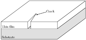
Figure 1.7: Channel crack in a thin film lying on top of a substrate. In this example
the substrate and the interface are intact.
- Delamination: As described in Section 1.3.1 the TSV structure is comprised of many
different materials. Delamination can evolve at the interface of two materials. Typically, an
interface crack nucleates from a site of high stress concentration such as a free edge of the
film or a geometric or material junction in a patterned structure. Residual stresses in the
films can be the cause of the crack interface propagation. The Figure 1.8 shows an
example of an interface crack.
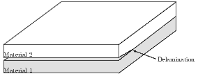
Figure 1.8: Interface crack between two materials. This phenomenon is also known
as delamination.
- Ratcheting: Interconnect materials under temperature cycling can exhibit failures such as
delamination, cracking, or metal film crawling. The cause of these failures is due to
the thermal expansion mismatch between the metal and the isolation material
or Si, causing a plastic deformation of the metal film. Directed by the shear
stresses, generated during various thermal cycles, the metal films introduce a
small amount of plastic deformation in each thermal cycle. After many thermal
cycles, the accumulated deformation is very large and it can cause a failure in
the device. For example, in Figure 1.9 the gray area indicates a packaging
material, the black area an isolating material, the orange area a substrate, and the
white area a metal. If we assume that the packaging material has a larger CTE
than the other materials, during the thermal cycle a shear stress (τ) will be
generated and transmitted to the metal material. It may appear that, after several
temperature cycles, the shear stress in the metal vanishes and the structure
plastically deforms. Over time this process can lead to a failure due to high material
deformation.
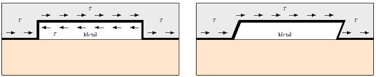
Figure 1.9: Ratcheting. The picture on the left indicates the structure before metal
deformation. The picture on the right denotes the deformed structure after many
thermal cycles.
- Electromigration: During its operation the interconnect line can carry a high electric
current. Due to this high current, metal atoms are transported in the direction of electron
flow inducing a wear-out of the interconnect metal (cf. Figure 1.10). This wear-out
mechanism normally leads to the formation of a void which grows and triggers a device
failure.
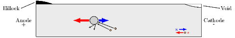
Figure 1.10: Schematic representation of the electromigration phenomenon. The
conducting electrons transfer the momentum to the metal ions. This causes the
gradual movement of ions and the formation of voids and consequently hillocks in
the conductor material.
- Stress-induced voiding: This refers to a break in a metal line or a via-hole occurring in
the absence of a current flow. As a result of multiple thermal cycles the material is
under different stresses which can cause the growth of a void, as presented in
Figure 1.11. So far, there is not a unanimously accepted theory of the stress-induced
voiding phenomenon. However, in copper structures it is thought to be due to the
high temperature processing. After the thermal process the copper has a large
tensile stress due to a mismatch in the CTEs of the materials involved and
therefore the stress relaxes in time through atom diffusion and thus by forming
voids.
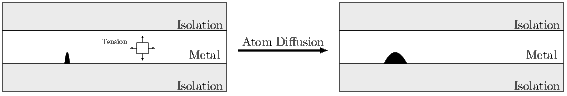
Figure 1.11: Due to a high stress the voids form and can increase in size leading to
an open circuit failure.
The finite element method (FEM) (also called finite element analysis (FEA)) is a numerical
method for solving a system of partial differential equations (PDEs). Most physical problems
(fatigue, electromigration, thermally induced failure mechanism, delamination, etc.) can be
described using a set of PDEs. FEM is employed to solve these PDEs and obtain an accurate
analysis of many different physical problems [32].
In a continuum problem of any dimensions an unknown field variable (displacement,
potential, etc.) has infinitely many values because it is a continuous function of generic points in
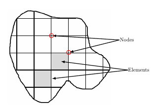
the body that generates an infinite number of unknowns. The main idea of FEM is to discretize
a domain into a finite number of elements in a way that the entire domain is approximated by
the union of these discrete elements (cf. Figure 1.12). The discretization procedure permits the
study of a field variable by reducing a problem to a finite number of unknowns field
variables.
The unknown field variable is expressed by assuming approximating functions (interpolation
functions) within each element. At specified nodes or nodal points of the domain, the
approximating functions are defined in terms of values of the field variables which are the
fundamental unknowns. Nodes are usually located on the element boundaries, where adjacent
elements are connected (cf. Figure 1.12). The behavior of the field variable within the
elements is described by the nodal values of the field variable and the interpolation functions.
The nodal values of the field variable are the new unknowns and they represent the finite
element problem. When these unknowns are obtained, the interpolation functions define the field
variable throughout the aggregated elements. Thus, the solutions are initially formulated
for individual elements and subsequently assembled to represent the entire problem
geometry [34].
FEM is widely employed in microelectronics. A multitude of different physical phenomena
can be handled by choosing the desired geometry and using the material data required. The
FEM tool permits the determination or prediction of the stress limits, or the lifetime of specific
configurations, fundamental for the reliability study.
In this document a detailed analysis of the mechanical failure of open TSV is presented. Finite
element simulations are employed to investigate the possible causes which lead to mechanical
failure. Different simulation schemes, material, and mechanical models are applied. By means of
simulations, different scenarios are studied leading to a comprehensive analysis of
the mechanical behavior of TSVs. The goal of this work is to improve and analyze
the reliability of the TSV interconnections and thus of the entire device leading to
a deeper understanding of TSVs. The study can help developers to improve their
processes.
The dissertation is divided into six chapters, including this introductory chapter,
Chapter 1. In Chapter 2 the elements of the linear elasticity theory are explained, followed
by the description of the FEM theory. Chapter 3, Chapter 4, and Chapter 5 present the
physical models employed and implemented to investigate the failure sources and
mechanisms in open TSVs. The stress evolution in an open TSV during 3D IC stacking is
analyzed in Chapter 3. The results presented in the Chapter 3 provide description of
the critical stress areas in an open TSV due to an external force. In these critical
areas a high probability of delamination failure is expected and therefore a study
of the delamination between these specific material layers in TSVs is presented in
Chapter 4. The probability of delamination is high in material films with high residual
stress. In Chapter 5 the generation of the intrinsic stress inside the metal films is
investigated. Chapter 6 summarizes the entire work and presents an outlook for further
studies.