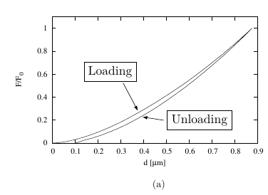
Figure 3.1: (a) A sample of load displacement curve. (b) An indenter penetrating in to a
sample.
In open TSVs the presence of high levels of mechanical stress is critical to the mechanical stability of the structure. During 3D IC stacking external mechanical stress acting on the TSV can be generated leading to accelerated circuit failure.
In this work an external force applied on an open TSV was reproduced using a model, which was implemented using FEM. The implemented model was calibrated using experimental data from an industrial partner. Subsequently the areas in the structure, in which a mechanical failure due to an external force is most likely, were localized. In these critical areas the probability of cracking or delamination is highest.
In the first part of this chapter a brief description of the approach used to reproduce an external force acting in open TSVs is provided. In the second part the results obtained from the FEM simulations are discussed.
During the 3D IC stacking, dies and wafers are bonded to each other, either as die-to-die, die-to-wafer, or wafer-to-wafer [14]. Different sources of mechanical stress can be identified during stacking:
In this work, these stresses are considered as an external load acting on an open TSV. During the stacking process mechanical stress evolves in the TSV structure, generating mechanical instability.
The approach used in order to treat the potential presence of unintentional indenters during bonding with open TSVs was the nanoindentation. Usually, nanoindentation is employed to evaluate the elastic modulus, the strain-hardening exponent, the fracture toughness, and the viscoelastic properties [38, 55]. However, in this study, nanoindentation was differently used. It was employed to reproduce an external load acting in an open TSV. This external load can result in additional mechanical stress during the 3D IC stacking. Nanoindentation is a simple method which consists of contacting the material of interest (open TSV) with another material (indenter). In one of these two materials, the mechanical properties, such as elastic modulus and hardness, are unknown. In the other, the material properties are known.
The main goal of this work was to estimate the areas in which mechanical failure due to an external load can be expected. From the results, a better understanding of how to increase the mechanical stability of the system can be obtained.
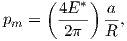
During nanoindentation, an indenter is placed in contact with the surface of a sample in which a steadily increasing load is applied. This causes the indenter to penetrate into the sample. Indenters can be adapted to suit the parameters under investigation and can therefore have different shapes and can be composed of different materials. Indenters are identified as spherical, conical, Vickers, or Berkovich [38, 56]. The applied force at the indenter is usually in the millinewton range, and the depth of penetration is on the order of micrometers.
During nanoindentation experiments, both load and depth of penetration are recorded at each load increment, resulting in load-displacement curves. Following the measurement of the maximum load, the indenter is steadily removed and the penetration depth is recorded again. If a residual impression is left on the surface of the specimen, a plastic deformation in the material has occurred. In contrast, if the removal of the indenter does not leave an impression, the material has behaved elastically.
Generally speaking the indentation stress-strain response of an elastic-plastic solid can be
divided into three regimes. These regimes are defined by considering the mean contact pressure
of the indenter
 | (3.1) |
where
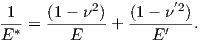 | (3.2) |
If the contacting bodies are two spheres, the indenter radius
 | (3.3) |
where
1
The three regimes during the nanoindentation are defined as [58]:
During these three regimes different physical phenomena may occur in the sample. Non-linear
events, such as phase transformation (
The mechanical reliability of TSVs is strongly connected to the material properties and the size of the device. Materials behave differently under mechanical stress, which affects the mechanical stability of the entire system. The bottom portion of an open TSV can be composed of different material layers. During the deposition processes and subsequent fabrication steps (die bonding, etc.), new mechanical stresses can be generated leading to mechanical instability. Mechanical stresses, in turn, determine the formation of new defects or the propagation of existing defects in the structure. Therefore, the material properties and the device geometry must be optimized in order to minimize mechanical stresses and to improve reliability [59].
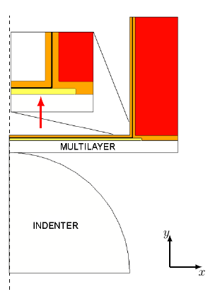
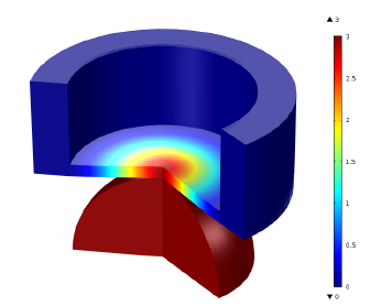
FEM was used to simulate the application of an external load on an open TSV, as shown in
The bottom of the TSV under consideration consists of a multilayer structure which
corresponds to the Al based interconnect structure for CMOS technology [29]. These layers are
materials with different thicknesses and mechanical properties. In the following, this
many-layered structure is diagrammatically depicted as a single layer, denoted as
“multilayer” in
The mechanical and electromechanical properties of the materials play an important role for the reliability of devices. Mechanical properties of thin films should be accurately measured at the length scale of the devices under consideration, since their properties are different from those of bulk materials. These differences can be due to size effects, grain structures, and processing [61]. Unfortunately material properties for thin materials employed in open TSV are not available in literature.
In an open TSV, the indenter can be placed at two different locations, either internal or external
to the TSV. These two locations will produce a different distribution of mechanical stress inside
the TSV. In this work an indenter acting external to an open TSV, as shown in
The simulations were performed by accounting for each material of the multilayer, rather
than considering a single artificial one (
FEM simulation requires a contact condition between indenter and sample to recreate the interaction between TSV bottom and indenter during penetration. In the implemented model, this condition was reproduced by employing the contact pressure penalty method [38, 62].
Accurate results are obtainable by modeling the contact areas of the indenter and the TSV
with a very fine mesh. In general, all geometries would benefit from a fine mesh, but this would
lead to excessively long simulation times. A mapped mesh with a minimum element size
of 0.5
A stationary parametric sweep study was performed. The movement of the indenter was emulated using the prescribed displacement as variable. This was repeated for increasing displacement, until the maximum measured displacement from the experimental data was reached.
The TSV structure was mechanically fixed at a single point, the top of the TSV sidewall. For the outer-rightmost Si region, a so-called roller constraint was chosen, which allows the material to move tangential to the boundary but not perpendicular to it. On the other edges, the TSV was free to move, allowing for a reproduction of the real conditions of the device.
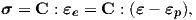
In the implemented model, the elastic-plastic behavior of the materials was considered. The elastic behavior was reproduced with Hooke’s law (2.37). The plastic behavior was described by employing an isotropic hardening law [62, 63].
An elastic-plastic material is usually modeled under the assumption that the strains
 | (3.4) |
where
When considering an isotropic plastic material, the strain increment is studied by using the
plastic potential
 | (3.5) |
where the three invariants are defined by
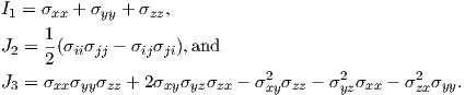 | (3.6) |
An increment of the plastic strain tensor 
 | (3.7) |
where 

 | (3.8) |
In the theory of plasticity, it is possible to describe yielding in the terms of
 | (3.9) |
where
The yield function is defined as
 | (3.10) |
where
Not only do the material parameters influence the load-displacement curves, but nanoindentation is also sensitive to the level of residual stress in the layers. The results of experimental indentation are therefore the sum of two contributions: plastic deformation and residual stress.
The model calibration can permit to understand how mechanical stress develops within
the different layers (multilayer) as the force applied by the indenter increases. The
presented model was calibrated using experimental data from an industrial partner. The
experimental data were obtained for a displacement of the indenter into the surface up
to approximately 3
In
From the experimental data it was possible to obtain the load-displacement curve. The loading plot provides information about the mechanical properties, as well as the failure of the device.
In
The results of the simulation are in good agreement with experimental data, as can be seen
in
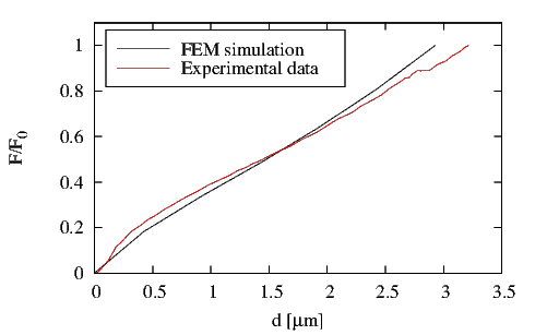
During the deposition processes, residual stresses develop in the layers of the multilayer structure. These stresses can influence the nanoindentation test [38]. Different values of residual stress [67] were attempted in thin films of the multilayer in order to assist the calibration process. However, these tests did not improve the fitting; therefore, the influence of the residual stress was not considered.
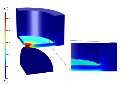
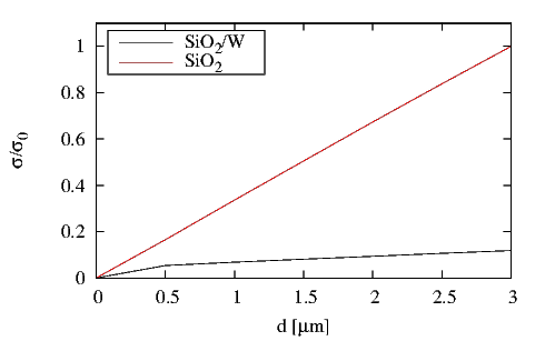
An increase in the displacement of the indenter increases the stress in the TSV. The inset
in
From the simulations stress values at different locations were determined allowing to deduce which mode of failure is most likely to occur. The highest stresses were found at the corner of the TSV sidewall, in particular:
The
In this chapter the stress development in the layers of open TSVs, during the application of an external force, was investigated. The implemented model permits to simulate the penetration of an indenter into the bottom of the TSV, reproducing the extra mechanical stress which might appear during the 3D IC stacking. The simulations were calibrated with experimental data, provided by an industrial partner. The model was fitted qualitatively by altering the plasticity parameters of the material under test. The simulations can predict the areas of the device in which there is increased stress and thereby a higher probability of failure. The following scenarios were found:
The model can be used to identify the way in which geometric and material properties influence the mechanical stability of TSVs during 3D IC stacking.