Previous: 2.1.2 Hybrid Integration and Intelligent Power Modules Up: 2.1 Power Devices Overview Next: 2.2 Lateral High-Voltage Devices for Smart Power Applications
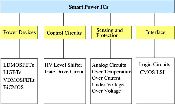
Monolithic integration of output power semiconductors with digital and analog circuitry includes power devices, signal processing and sensing (and protection) circuits on the same chip. Monolithic solutions for power conversion and amplification are highly desirable not only for the reduction of interfaces, and thus volume, weight and electromagnetic interferences, but also for increasing efficiency, performance and reliability of the overall system. A wide range of applications is predictable for these monolithic solutions, since the power delivered by a power IC (PIC) into a load can be tens and even thousands of watts. Many approaches are being investigated to search for new strategies to reduce the cost of PICs [39]. There are two types of PICs, HVICs and smart power.
HVICs are designed to deliver low output currents (up to 100mA) at supply voltages up to 1000V. They typically find applications in automobiles, electrostatic and ink-jet printers, and plasma displays. In HVICs the VLSI circuit is improved by output buffers that consist of low-current integrated power devices with coplanar electrodes like CMOS compatible high-voltage MOS devices.
The term smart power is usually used to define power integrated circuits which provide the interface between the digital control logic and the power load, aimed to control the power of the system (up to a few hundreds of volts and a few amperes). This fact motivated the development of sophisticated and rather costly technologies that permit to merge in the same chip power devices together with control, protection, and sensing circuitry, as well as microprocessor interfacing and fault diagnosis.
Smart power technology is aimed of performing complex switching functions at high frequencies, motivating progress in this area, and pushing manufacturers to launch application-specific PICs into the market, for low or medium power, namely for automobile industry, robotics, portable telecommunication and medical equipment, display driver ICs [67,68,69,70], areas which call for high reliability [71] and compactness. The impact of smart power technology on the recent advances in automobile and aerospace industries, and telecommunications equipments is remarkable. A drastic cost reduction is possible by applying these monolithic solutions to many consumer products, such as home appliances, air-conditioners, lighting systems, machine-tools, and robotics.
One of the main features of smart power technologies
relates to the isolation techniques used between the power part and
the low-voltage IC part [61,72].
The isolation between the power part and the low-voltage part is achieved
by JI technologies or dielectric isolation. The traditional approach
of the industry is to use the JI for cost reduction.
The conventional dielectric isolation with polysilicon deposited as a
substrate layer is very expensive.
Over the last years a cheaper solution based on SOI wafers
has been developed. However, a development of this kind of
isolation is linked to cost reduction.
Thus, isolation by means of a junction remains the preferred solution
for standard applications, whereas the dielectric isolation is being used
for specific applications requiring a high level of isolation.
The major fields of application of these PICs
are portable equipment, domestic appliances, lighting, and the
automotive industry.
The development of PICs has been essentially driven by the automotive
electronic requirement for applications such as motor control and fuel injector drivers.
The choice of a structure of power devices, the level of integration, and the
isolation technique are based on the type of application and, therefore,
on the power range desired. However, the best performance of the power
component is considered (normally
![]() and BV trade-off) as well as the highest
level of integration of the detection, control, and protection elements.
and BV trade-off) as well as the highest
level of integration of the detection, control, and protection elements.
Smart power devices have always used design rules and technologies
which are less efficient than that used for ULSI and VLSI devices.
In the early eighties the first smart power
devices were fabricated with 2.5 or 4![]() m design rules while ULSI used
1
m design rules while ULSI used
1![]() m design rules. When ULSI devices used submicron IC design
rules smart power devices were fabricated with 1.5 or 2
m design rules. When ULSI devices used submicron IC design
rules smart power devices were fabricated with 1.5 or 2![]() m design rules.
This difference was essentially linked (i) to the more
complex fabrication that must be taken into account: isolation, edge
terminations for power devices, combination of different kinds of devices,
CMOS, DMOS, bipolar, and (ii) to the important development of VLSI and ULSI
devices driven by a large market.
The technology developed for ULSI and VLSI circuits has always been
used a few years later for smart power devices.
m design rules.
This difference was essentially linked (i) to the more
complex fabrication that must be taken into account: isolation, edge
terminations for power devices, combination of different kinds of devices,
CMOS, DMOS, bipolar, and (ii) to the important development of VLSI and ULSI
devices driven by a large market.
The technology developed for ULSI and VLSI circuits has always been
used a few years later for smart power devices.
Recently design rules for smart power devices went down from 0.8 to 0.35![]() m,
which offers the possibility of integration of smart power
ICs. This strong drive towards integration leads to single
chip system for low power applications.
Some manufacturers prefer a mixed technology. However, overall design rules do
not help to reduce the device area, because most of the
chip size is determined by the power device parts. This must be considered
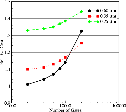
in the manufacturing costs. Figure 2.7 shows the cost trend of lithography
technology [73].
If the number of gates is roughly below 10000, 0.6
m,
which offers the possibility of integration of smart power
ICs. This strong drive towards integration leads to single
chip system for low power applications.
Some manufacturers prefer a mixed technology. However, overall design rules do
not help to reduce the device area, because most of the
chip size is determined by the power device parts. This must be considered
in the manufacturing costs. Figure 2.7 shows the cost trend of lithography
technology [73].
If the number of gates is roughly below 10000, 0.6![]() m technology is
the cheaper solution compared to the 0.35
m technology is
the cheaper solution compared to the 0.35![]() m design rule.
Many low-power blocks can be introduced on a single chip.
By reducing the number of interconnections in chips, assembly costs are
also lowered and the system becomes more reliable.
In order to minimize design time, libraries for logic and analog
blocks can be used. However, improvement essentially concerns the power device.
Indeed, improvements of the power device performances (
m design rule.
Many low-power blocks can be introduced on a single chip.
By reducing the number of interconnections in chips, assembly costs are
also lowered and the system becomes more reliable.
In order to minimize design time, libraries for logic and analog
blocks can be used. However, improvement essentially concerns the power device.
Indeed, improvements of the power device performances (
![]() and BV)
have been limited ever since the introduction of the 1.4
and BV)
have been limited ever since the introduction of the 1.4![]() m technology.
So, new structures are needed to enhance
performance (SJ devices [74,75,76,77,78,79], LUDMOS [16],
and multi-channel [35]).
m technology.
So, new structures are needed to enhance
performance (SJ devices [74,75,76,77,78,79], LUDMOS [16],
and multi-channel [35]).
Jong-Mun Park 2004-10-28