Previous: 2.2.1 Lateral DMOSFETs Up: 2.2 Lateral High-Voltage Devices for Smart Power Applications Next: 2.2.3 Lateral MCTs
The major limitation of LDMOSFETs is their relatively
high specific on-resistance
![]() due to the majority carrier conduction mechanism.
The Insulated Gate Bipolar Transistor (IGBT) is a relatively new power device
which is designed to overcome the high on-state loss of power MOSFETs.
The device is essentially a combination of a
due to the majority carrier conduction mechanism.
The Insulated Gate Bipolar Transistor (IGBT) is a relatively new power device
which is designed to overcome the high on-state loss of power MOSFETs.
The device is essentially a combination of a ![]() -bipolar transistor
which provides high current handling capability, and an
-bipolar transistor
which provides high current handling capability, and an ![]() -channel MOSFET
which gives a high-impedance voltage control over the bipolar base current.
It can be fabricated both as a high-power discrete vertical IGBT and a low-power
lateral IGBT, the latter of which presents interesting possibilities for
integration together with control circuitry.
-channel MOSFET
which gives a high-impedance voltage control over the bipolar base current.
It can be fabricated both as a high-power discrete vertical IGBT and a low-power
lateral IGBT, the latter of which presents interesting possibilities for
integration together with control circuitry.
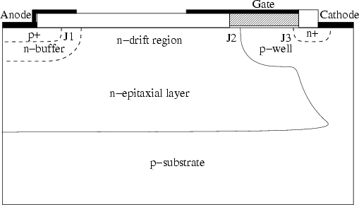
Figure 2.12 shows a cross section of an LIGBT.
The structure of the LIGBT is similar
to that of an LDMOSFET, the gate is also formed by double diffusion.
The main difference between this structure and an LDMOSFET
is that it has a ![]() -anode instead of the
-anode instead of the ![]() -drain of LDMOSFETs.
In this structure current flow cannot occur when a negative voltage is
applied to the anode with respect to the cathode, because the emitter
junction J1 (junction between anode and
-drain of LDMOSFETs.
In this structure current flow cannot occur when a negative voltage is
applied to the anode with respect to the cathode, because the emitter
junction J1 (junction between anode and ![]() -buffer) becomes
reverse biased. This provides the device with its reverse blocking state, and
the depletion region extends in the
-buffer) becomes
reverse biased. This provides the device with its reverse blocking state, and
the depletion region extends in the ![]() -drift region.
When a positive voltage is applied to the anode with the gate shorted
to the cathode, J2 (
-drift region.
When a positive voltage is applied to the anode with the gate shorted
to the cathode, J2 (![]() -drift and
-drift and ![]() -well junction) becomes reverse biased and
the device operates in its forward blocking state.
Generally, the substrate is electrically connected to the source contact.
When a positive gate voltage above the threshold voltage is applied with
respect to the cathode (source), an inversion channel is formed that connects
the
-well junction) becomes reverse biased and
the device operates in its forward blocking state.
Generally, the substrate is electrically connected to the source contact.
When a positive gate voltage above the threshold voltage is applied with
respect to the cathode (source), an inversion channel is formed that connects
the ![]() -cathode to the
-cathode to the ![]() -drift region.
This creates the base current of the lateral
-drift region.
This creates the base current of the lateral ![]() -transistor in the
LIGBT structure.
If a positive voltage is applied between the
-transistor in the
LIGBT structure.
If a positive voltage is applied between the ![]() -anode and cathode,
most of the voltage drops across J1, until the junction becomes forward biased.
Under forward bias any additional increase in voltage drops across the channel and the drift
region. The holes from the anode are injected into the
-anode and cathode,
most of the voltage drops across J1, until the junction becomes forward biased.
Under forward bias any additional increase in voltage drops across the channel and the drift
region. The holes from the anode are injected into the ![]() -drift region and
electrons flow into the drift region from the source through the channel.
Because of the injected electrons and holes, the
-drift region and
electrons flow into the drift region from the source through the channel.
Because of the injected electrons and holes, the ![]() -drift region becomes
conductivity modulated. With further increase in the anode voltage,
more voltage drops across the inversion channel and the electron
current increases to compensate for the increased hole current.
If the hole concentration exceeds the background doping level of the
-drift region becomes
conductivity modulated. With further increase in the anode voltage,
more voltage drops across the inversion channel and the electron
current increases to compensate for the increased hole current.
If the hole concentration exceeds the background doping level of the
![]() -drift region, the device characteristics are similar to those
of a forward biased
-drift region, the device characteristics are similar to those
of a forward biased ![]() -diode. As a result, it can be operated at a higher
current density compared to conventional LDMOSFETs.
-diode. As a result, it can be operated at a higher
current density compared to conventional LDMOSFETs.
If the inversion layer conductivity is reduced by the gate bias close to the threshold voltage, a significant voltage drop occurs across the channel. When this voltage drop becomes comparable to the difference between the gate bias and the threshold voltage, the channel is pinched-off. At this point, the electron current saturates. As a result, the device operates with current saturation in its active region with a gate controlled output current. In order to switch off the device, it is necessary to discharge the gate by shorting it to the cathode.
When the gate to cathode voltage is reduced to zero, the device
is switched from its on-state to off-state, the current will fall
to a fraction of the steady state value due to the cut-off of the
electron current. This will be followed by a slow decay of the
anode current over a long period of time.
In the second phase, the carriers are removed mainly by electron-hole
recombination as there is no other efficient way to extract
the minority carriers from the drift region. The turn-off time therefore
depends on the lifetime of the minority carriers.
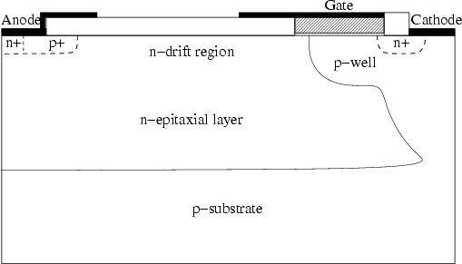
An improvement in the turn-off time of the LIGBT can be achieved by
incorporating a shorting ![]() -diffusion at the anode to create a
shorted-anode structure. The addition of this shorting diffusion
results in more efficient removal of electrons thereby decreasing
the turn-off time. The
-diffusion at the anode to create a
shorted-anode structure. The addition of this shorting diffusion
results in more efficient removal of electrons thereby decreasing
the turn-off time. The ![]() -anode short provides an electron
extraction path during turn-off.
-anode short provides an electron
extraction path during turn-off.
Figure 2.13 shows the schematics of the shorted-anode LIGBT (SA-LIGBT).
As shown in the figure the device has a hybrid LDMOSFET-LIGBT structure
with a common drift region. It allows a much higher current density compared to the
LDMOSFET because of the conductivity modulation at the drift region
and faster switching speed compared to the conventional LIGBT by the electron
path during turn-off. It has a negative differential resistance region which is
undesirable for device operation. This is due to the two different
conduction mechanisms responsible for the current flow depending on the
bias conditions. At low anode voltages the device exhibits MOSFET like operation.
As the anode voltage increases, the ![]() -anode and the
-anode and the ![]() -drift junction becomes
forward biased. In addition hole injection from the
-drift junction becomes
forward biased. In addition hole injection from the ![]() -anode to the
-anode to the ![]() -drift takes place,
resulting in a smaller forward voltage drop by the bipolar operation.
-drift takes place,
resulting in a smaller forward voltage drop by the bipolar operation.
LIGBTs are susceptible to latch-up in the same way as discrete IGBTs because
of an inherent parasitic ![]() -thyristor in the device. At high
current levels the voltage drop across the cathode-body junction is
sufficient to turn the parasitic
-thyristor in the device. At high
current levels the voltage drop across the cathode-body junction is
sufficient to turn the parasitic ![]() -transistor on.
The collector current of the
-transistor on.
The collector current of the ![]() -transistor forms the base current
for the lateral
-transistor forms the base current
for the lateral ![]() -transistor. When the sum of the current gains of the
two transistors reaches unity, latch-up occurs and gate control is lost.
In a RESURF device a parasitic vertical
-transistor. When the sum of the current gains of the
two transistors reaches unity, latch-up occurs and gate control is lost.
In a RESURF device a parasitic vertical ![]() -transistor is also formed
by substrate,
-transistor is also formed
by substrate, ![]() -layer and the
-layer and the ![]() -well which diverts some of the current
and the latch-up threshold is increased.
One method to suppress latch-up is aimed at lowering the gain of
the
-well which diverts some of the current
and the latch-up threshold is increased.
One method to suppress latch-up is aimed at lowering the gain of
the ![]() -transistor by using a
-transistor by using a ![]() -buried layer and a deep
-buried layer and a deep ![]() -sinker
together with the
-sinker
together with the ![]() -buffer layer at the cathode region (see Figure 2.12).
This
-buffer layer at the cathode region (see Figure 2.12).
This ![]() -buffer can help to reduce charge injection by controlling
the emitter efficiency of the device.
-buffer can help to reduce charge injection by controlling
the emitter efficiency of the device.
Jong-Mun Park 2004-10-28