Previous: 2.2.3 Lateral MCTs Up: 2.2 Lateral High-Voltage Devices for Smart Power Applications Next: 2.3 RESURF
LDMOSFETs have a high switching speed and low switching losses but
a relatively low current density in the on-state.
On the other hand, IGBTs offer high current densities because of
conductivity modulation in the drift region, but have poor switching
performance compared to LDMOSFETs. Excess carriers in the
drift region generate a tail current in the off-state, which can be
removed only by recombination processes. By introducing extra
![]() -doping in the anode (anode-shorted structure) of the LIGBT the switching
performance can be improved drastically, but the anode-shorted
LIGBT has an inherent snapback characteristic which is not attractive
from a circuit design point of view.
-doping in the anode (anode-shorted structure) of the LIGBT the switching
performance can be improved drastically, but the anode-shorted
LIGBT has an inherent snapback characteristic which is not attractive
from a circuit design point of view.
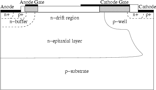
The dual gate lateral inversion layer emitter transistor (DGLILET) is a device that offers controlled carrier injection and fast switching performance. Figure 2.15 shows the cross section of the device. The combination of a shorted-anode structure and an extra gate at the anode gives high switching speed while suppressing the undesirable snapback characteristics. The cathode gate performs the role of the main control gate like in the case of LIGBTs and the anode gate controls carrier injection.
The anode gate which is driven negative with respect to the anode, forms
an inversion layer of holes. The flow of electron current underneath the
hole inversion layer initiates minority carrier injection driving the device into
conductivity modulation.
Having the inversion layer in the high resistance ![]() -drift region initiates
the injection at a very low current density, suppressing the snapback.
Moreover, the anode gate acts as a field plate improving
the voltage blocking capability of the device.
-drift region initiates
the injection at a very low current density, suppressing the snapback.
Moreover, the anode gate acts as a field plate improving
the voltage blocking capability of the device.
Full control over hole injection into the device drift region can be
achieved by minimizing the length of the ![]() -anode diffusion.
This prevents the potential drop due to lateral electron current flow
beneath the
-anode diffusion.
This prevents the potential drop due to lateral electron current flow
beneath the ![]() -diffusion becoming large enough to forward bias the
-diffusion becoming large enough to forward bias the
![]() -diffusion and
-diffusion and ![]() -well junction at normal operating current densities.
This ensures that injection is taking place only at the hole inversion
layer, and thus the anode gate has full control of injection.
The device can therefore be switched between unipolar and
bipolar modes of conduction. Switching the anode gate off slightly
before the actual turn off of the device suppresses injection and improves
the turn-off speed of the device.
On the other hand, the
-well junction at normal operating current densities.
This ensures that injection is taking place only at the hole inversion
layer, and thus the anode gate has full control of injection.
The device can therefore be switched between unipolar and
bipolar modes of conduction. Switching the anode gate off slightly
before the actual turn off of the device suppresses injection and improves
the turn-off speed of the device.
On the other hand, the ![]() -diffusion can be designed to allow injection
of holes into the
-diffusion can be designed to allow injection
of holes into the ![]() -well at a higher current density. The injection of holes
is initially established by the hole inversion layer and the injection
from the
-well at a higher current density. The injection of holes
is initially established by the hole inversion layer and the injection
from the ![]() -diffusion is commenced at a latter stage conserving
the snapback suppression.
In this design turning off the anode gate before cathode gate might not
suppress the injection depending on the operating current density.
The on-state is improved due to a higher level of modulation but
the turn-off time will be slightly increased.
-diffusion is commenced at a latter stage conserving
the snapback suppression.
In this design turning off the anode gate before cathode gate might not
suppress the injection depending on the operating current density.
The on-state is improved due to a higher level of modulation but
the turn-off time will be slightly increased.
Jong-Mun Park 2004-10-28