Previous: 3.1.3 Carrier Recombination and Generation Up: 3.1 Transport Physics Considered for Power Semiconductor Devices Next: 3.1.5 Impact Ionization
The carrier lifetime (recombination lifetime) is defined as the average
time it takes an excess minority carrier to recombine.
As mentioned in the previous section, three recombination mechanisms -
band-to-band, trap-assisted (or SRH) and Auger recombinations - determine the
recombination lifetime.
Band-to-band recombination is relatively unimportant in silicon, because its radiative
lifetime is extremely high. Auger lifetime is independent of any impurity
density. However, it is inversely proportional to the carrier density. SRH recombination
is determined by the amount of impuities and defects in the silicon.
Therefore, at high carrier densities, the recombination lifetime in silicon is controlled
by Auger recombination and at low carrier densities by SRH recombination.
The minority carrier lifetime in heavily
doped ![]() - and
- and ![]() -type material is related to the capture rate for electrons
and holes at the recombination center. In addition it is a function of the doping
concentration, because additional traps are created at high doping level.
-type material is related to the capture rate for electrons
and holes at the recombination center. In addition it is a function of the doping
concentration, because additional traps are created at high doping level.
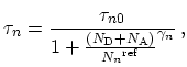
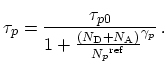
For the SRH recombination the minority carrier
lifetimes ![]() and
and ![]() can be shown as:
can be shown as:
 |
(3.17) |
 |
(3.18) |
where
![]() ,
,
![]() ,
, ![]() , and
, and ![]() are fitting parameters for
electrons and holes, respectively [18].
are fitting parameters for
electrons and holes, respectively [18]. ![]() and
and ![]() are the
electron and hole minority carrier life times at low doping levels, respectively.
The carrier lifetime is very sensitive to
the fabrication procedure, and it is very difficult to determine
this value without any measurement data. One way to determine
the lifetime is to measure the capture cross-sections and the
positions of the recombination (deep level) center in the band gap.
At low injection levels the lifetime
are the
electron and hole minority carrier life times at low doping levels, respectively.
The carrier lifetime is very sensitive to
the fabrication procedure, and it is very difficult to determine
this value without any measurement data. One way to determine
the lifetime is to measure the capture cross-sections and the
positions of the recombination (deep level) center in the band gap.
At low injection levels the lifetime
![]() depends on the deep level
position in the band gap and the capture cross-section ratio
depends on the deep level
position in the band gap and the capture cross-section ratio ![]()
![]()
![]()
![]()
![]() .
.
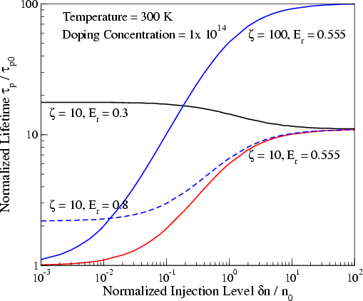
Figure 3.3 shows the variation in the lifetime with normalized
injection level ![]()
![]()
![]() (where
(where ![]() is an excess electron concentration and
is an excess electron concentration and
![]() is an equilibrium concentration of electron) for the
is an equilibrium concentration of electron) for the ![]() -type
silicon for doping concentration of 1
-type
silicon for doping concentration of 1 ![]()
![]()
![]() .
In Figure 3.3, capture cross-section ratio
.
In Figure 3.3, capture cross-section ratio ![]() and
deep level in the energy gap
and
deep level in the energy gap
![]() are considered.
At low injection level (
are considered.
At low injection level (![]()
![]()
![]()
![]() 1) the lifetime is dependent upon the deep
level position
1) the lifetime is dependent upon the deep
level position
![]() and capture cross-section ratio
and capture cross-section ratio ![]() .
It has a minimum when the recombination center lies close
to middle of the band gap (
.
It has a minimum when the recombination center lies close
to middle of the band gap (
![]()
![]() 0.555 in Figure 3.3).
On the other hand, the high level lifetime
0.555 in Figure 3.3).
On the other hand, the high level lifetime
![]() approaches a constant value. It is not dependent upon the position of the deep level,
but it depends on the capture cross-section ratio
approaches a constant value. It is not dependent upon the position of the deep level,
but it depends on the capture cross-section ratio ![]() [59]
[59]
 |
(3.19) |
The recombination rates of majority carriers equals that of minority carriers, because a recombination process involves an equal number of holes and electrons.
The generation lifetime ![]() in a space charge region where the hole and
electron concentration are close to each other can be derived from the SRH
recombination generation equation
in a space charge region where the hole and
electron concentration are close to each other can be derived from the SRH
recombination generation equation
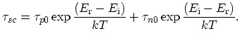 |
(3.20) |
For bipolar power devices a small low level lifetime is highly desirable to obtain fast switching performance. On the other hand, a large high level lifetime is desirable to obtain high current density during on-state. In addition a lower space charge generation lifetime produces a higher leakage current. For obtaining the best trade-off among the device characteristics, such as switching speed, on-state current, and leakage current, it is important to find an optimal location of a deep level position and its capture cross-section. Several methods can be applied to control the carrier lifetime of bipolar power devices (gold and platinum diffusions, electron or proton irradiations, gamma-ray irradiation, etc.).
The variation in the lifetime with temperature is also important for power devices operating at a high temperature. From measurements of the recombination lifetime in power devices it was concluded that the lifetime increases with rising temperature. We assume a simple power law for the temperature dependence of the carrier lifetime
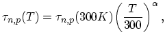 |
(3.21) |
where the coefficient
![]()
![]()
![]() 2.5 for high temperature simulations.
2.5 for high temperature simulations.
Jong-Mun Park 2004-10-28