Previous: 3.3 Super-Junction Concepts Up: 3.3 Super-Junction Concepts Next: 3.3.2 SJ -Diode
One of the major drawbacks of power MOSFETs compared to
bipolar devices is their high on-state conduction loss for
high-voltage applications.
Generally, power MOSFETs have a double-diffused structure with
a lightly doped drift region to support the high voltage.
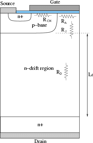
Figure 3.12 shows a standard power DMOSFET.
The on-resistance of the structure shown in the figure is the
total resistance between
the source and drain terminal in the on-state. This can be determined
by the resistance components of the device. The major resistance
components for high-voltage DMOSFETs are the channel (
![]() ), accumulation (
), accumulation (
![]() )
and drift layer (
)
and drift layer (
![]() ) resistances, and
) resistances, and
![]() which is the
contribution from the drift region between the
which is the
contribution from the drift region between the
![]() -base regions (JFET region).
The resistances of the
-base regions (JFET region).
The resistances of the ![]() -emitter and substrate regions are generally
negligible for high-voltage power MOSFETs. For high-voltage devices the drift region
contributes a large resistance. It is important to decrease the drift
doping concentration to obtain a high blocking voltage.
Increasing the BV can result in a significant
undesired increase of
-emitter and substrate regions are generally
negligible for high-voltage power MOSFETs. For high-voltage devices the drift region
contributes a large resistance. It is important to decrease the drift
doping concentration to obtain a high blocking voltage.
Increasing the BV can result in a significant
undesired increase of
![]() .
.
Consider the ideal case where the
![]() of power MOSFETs is determined
by the drift region only, and assume that the current flows uniformly
through the drift region without current spreading effects.
Then the relation between the on-resistance and the BV can be expressed as
of power MOSFETs is determined
by the drift region only, and assume that the current flows uniformly
through the drift region without current spreading effects.
Then the relation between the on-resistance and the BV can be expressed as
| (3.39) |
for ![]() -channel devices and
-channel devices and
| (3.40) |
for ![]() -channel devices. The resistances of the accumulation and JFET region
are not considered in the equations. The mobility of the drift region also
affects the on-resistance of the devices.
-channel devices. The resistances of the accumulation and JFET region
are not considered in the equations. The mobility of the drift region also
affects the on-resistance of the devices.
In deriving the numerical values in these equations, it is assumed that
the mobility is that for a relatively low doping
concentration (
![]() ).
The ideal
).
The ideal
![]() of a
of a ![]() -channel MOSFET is higher than that for
the
-channel MOSFET is higher than that for
the ![]() -channel MOSFET due to the lower mobility of holes than electrons in silicon.
-channel MOSFET due to the lower mobility of holes than electrons in silicon.
In low-voltage MOSFETs below 100V, the channel resistance and the charge accumulation layer resistance are the dominant factors in the total on-resistance of MOSFETs. These resistances account more than 80% of the total resistance in 20V class devices. On the other hand, in the medium- and high-voltage MOSFETs, the resistance is dominated by doping concentration and thickness of the drift region.
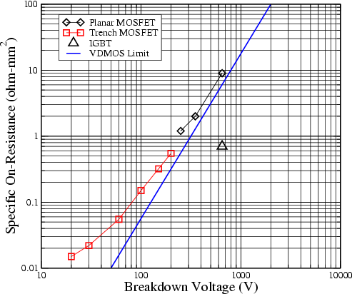
Figure 3.13 shows the state-of-the-art trade-off between
![]() and BV of standard power MOSFETs and theoretical silicon limit, respectively [133].
The superior switching performance of the power MOSFET ensure that it has become a
key device in the field of SMPS. However, as can be seen in the figure,
the on-resistance of power MOSFETs increases
sharply with the BV. This has prevented the use of power MOSFETs at high voltages.
A high blocking voltage of a standard power MOSFET requires a
thick and low doped epitaxial layer (
and BV of standard power MOSFETs and theoretical silicon limit, respectively [133].
The superior switching performance of the power MOSFET ensure that it has become a
key device in the field of SMPS. However, as can be seen in the figure,
the on-resistance of power MOSFETs increases
sharply with the BV. This has prevented the use of power MOSFETs at high voltages.
A high blocking voltage of a standard power MOSFET requires a
thick and low doped epitaxial layer (![]() -drift region)
which causes an increase in the on-resistance.
A variety of MOS structures can be used for power MOSFETs. In the medium- and high-voltage
applications, reliability and SOA (safe operating area) of the device are more
important than the on-resistance. Therefore, planar structure is frequently used in the
high-voltage power MOSFETs, and the trench structure is used in the low-voltage
MOSFETs (see Figure 3.13).
-drift region)
which causes an increase in the on-resistance.
A variety of MOS structures can be used for power MOSFETs. In the medium- and high-voltage
applications, reliability and SOA (safe operating area) of the device are more
important than the on-resistance. Therefore, planar structure is frequently used in the
high-voltage power MOSFETs, and the trench structure is used in the low-voltage
MOSFETs (see Figure 3.13).
Jong-Mun Park 2004-10-28