Previous: 3.3.2 SJ -Diode Up: 3.3 Super-Junction Concepts Next: 3.3.4 SJ SOI-LDMOSFETs
Vertical SJ DMOSFET were recently introduced both theoretically and commercially and
achieved a significant improvement in the trade-off between
![]() and BV compared to
conventional VDMOSFETs.
Vertical SJ devices such as COOLMOS [31] and MDmesh [32]
assume complete charge balance of the depletion layer. This can be achieved by
introducing alternating
and BV compared to
conventional VDMOSFETs.
Vertical SJ devices such as COOLMOS [31] and MDmesh [32]
assume complete charge balance of the depletion layer. This can be achieved by
introducing alternating ![]() - and
- and ![]() -columns in the drift region, which allows to
drastically increase the doping in this region.
A series of multiple epitaxial depositions of lightly
-columns in the drift region, which allows to
drastically increase the doping in this region.
A series of multiple epitaxial depositions of lightly ![]() -doped silicon on a highly
doped
-doped silicon on a highly
doped ![]() -substrate and related boron (and
-substrate and related boron (and![]() or phosphor) implantation steps can be used
for the fabrication of such vertical SJ devices. However, precise control of the mask steps is
important for this process.
Even the current conduction area is reduced by additional
or phosphor) implantation steps can be used
for the fabrication of such vertical SJ devices. However, precise control of the mask steps is
important for this process.
Even the current conduction area is reduced by additional ![]() -columns which
do not contribute towards on-state conduction, which results in a significant
reduction in
-columns which
do not contribute towards on-state conduction, which results in a significant
reduction in
![]() of the devices by using a high doping concentration in the
of the devices by using a high doping concentration in the ![]() -pillar.
-pillar.
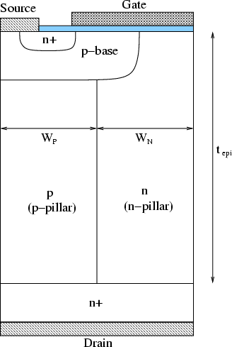
Figure 3.22 shows a cross section of a SJ DMOSFET, which has a
concept similar to a multi-RESURF idea. This structure allows a doping
level of the ![]() -region, which is typically one order of magnitude higher
than that in standard high-voltage MOSFETs. The additional charge is
counterbalanced by the adjacent charges of the
-region, which is typically one order of magnitude higher
than that in standard high-voltage MOSFETs. The additional charge is
counterbalanced by the adjacent charges of the ![]() -column, thus contributing
to a horizontal electrical field without affecting the vertical field
distribution.
The electric field inside the structure is fixed by the net charge of the two
oppositely doped columns. Thus a nearly flat field distribution similar to that
in SJ
-column, thus contributing
to a horizontal electrical field without affecting the vertical field
distribution.
The electric field inside the structure is fixed by the net charge of the two
oppositely doped columns. Thus a nearly flat field distribution similar to that
in SJ ![]() -structures can be achieved, if both regions
counterbalance each other perfectly.
-structures can be achieved, if both regions
counterbalance each other perfectly.
For higher blocking voltages only the depth of the columns has to be increased without
any change of the doping. This leads to a linear relationship between blocking
voltage and on-resistance instead of the power relationship for the case of conventional
VDMOSFETs.
Considering the drift region of a SJ DMOSFET has a length
![]() , the
, the ![]() - and
- and ![]() -column
widths are
-column
widths are
![]()
![]()
![]()
![]()
![]() ,
and the
,
and the ![]() - and
- and ![]() -column dopings are
-column dopings are
![]() and
and
![]() , respectively, and assuming that the
, respectively, and assuming that the ![]() - and
- and ![]() -pillars
are completely depleted before breakdown and perfect charge
balance of each column, the BV and the charge
-pillars
are completely depleted before breakdown and perfect charge
balance of each column, the BV and the charge
![]() of the column are given by
of the column are given by
| (3.41) |
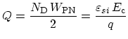 |
(3.42) |
where the critical electric field
![]() is also
increased by the increased doping concentration of the pillar.
is also
increased by the increased doping concentration of the pillar.
Because the current flows only through the ![]() -column,
the specific on-resistance
-column,
the specific on-resistance
![]() can be expressed as
can be expressed as
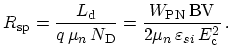 |
(3.43) |
This equation clearly shows the linear relationship between the BV and the specific on-resistance of SJ DMOSFETs instead of the power relationship for the case of conventional DMOSFETs.
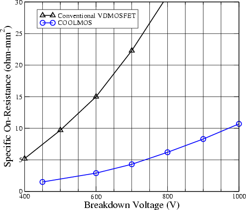
Figure 3.23 shows the
![]() comparison of the commercial COOLMOS
and VDMOSFET [134].
comparison of the commercial COOLMOS
and VDMOSFET [134].
![]() of the conventional VDMOSFET increases
sharply as a function of blocking voltage. COOLMOS (vertical super-junction
MOS transistor) has a week linear relationship between
of the conventional VDMOSFET increases
sharply as a function of blocking voltage. COOLMOS (vertical super-junction
MOS transistor) has a week linear relationship between
![]() and BV.
and BV.
Practically the main advantage of SJ DMOSFETs is the drastic reduction of the device area because of its low specific on-resistance. This small chip size of the SJ DMOSFET leads to a low gate charge, which results in a short turn-on delay time compared to that of conventional DMOSFETs with comparable voltage and current ratings.
Jong-Mun Park 2004-10-28