Previous: 4.2.2 Device Structures and Operations Up: 4.2 Lateral Trench Gate SOI-LDMOSFETs Next: 4.2.3.1 Off-State Characteristics and Self-Heating
Reducing the on-resistance while maintaining a desired BV
rating has been the main issue in the development of lateral power devices.
The on-resistance of high-voltage SOI-LDMOSFETs strongly depends on
the doping of the drift layer.
In order to increase the BV of RESURF devices the doping
of the drift layer must be reduced and the drift layer length increased.
![]() and BV are inversely related to each other.
and BV are inversely related to each other.
In conventional SOI-LDMOSFETs a large voltage drops in the buried oxide, and it prevents potential lines from spreading into the substrate. Because the maximum electric field strength of the buried oxide is determined by the electric field strength of silicon at the interface between the silicon and the buried oxide, in the thin film SOI almost all the voltage drops in the buried oxide layer. To achieve a higher BV the surface electric field must be reduced by optimizing the drift length and the doping.
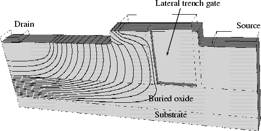
Figure 4.14 shows the potential distribution of the
lateral trench gate SOI-LDMOSFET at a drain-source
voltage of
![]() = 110V. The equipotential lines are uniformly
spaced along the surface of the drift region.
It exhibits a similar potential
distribution as that of the conventional device, the lateral
trench does not affect the RESURF condition. With the same
BV as the conventional device it helps to
decrease the on-resistance by increasing the current spreading
area at the channel region. Three-dimensional numerical
analysis have been performed to
investigate the BV,
= 110V. The equipotential lines are uniformly
spaced along the surface of the drift region.
It exhibits a similar potential
distribution as that of the conventional device, the lateral
trench does not affect the RESURF condition. With the same
BV as the conventional device it helps to
decrease the on-resistance by increasing the current spreading
area at the channel region. Three-dimensional numerical
analysis have been performed to
investigate the BV,
![]() , and self-heating effects as a
function of the lateral trench depth, and the space between the
trenches.
, and self-heating effects as a
function of the lateral trench depth, and the space between the
trenches.