Previous: 4.3.1 Introduction Up: 4.3 SJ Lateral Trench Gate SOI-LDMOSFETs Next: 4.3.3 Simulation Results
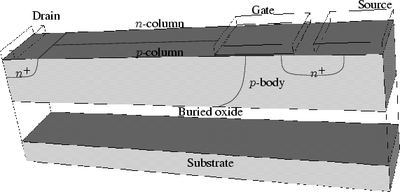
Figure 4.24 and Figure 4.25 show the schematic structures of a standard
SJ LDMOSFET on SOI and a proposed lateral trench gate SJ SOI-LDMOSFET
which are used for the simulation of the BV and the on-resistance, respectively.
As shown in Figure 4.24, the standard SJ SOI-LDMOSFETs can be made by
introducing extra ![]() -columns in the drift region. It is assumed that the charge in
the
-columns in the drift region. It is assumed that the charge in
the ![]() - and
- and ![]() -column of the drift layer should be exactly balanced, and this is true
only when the drift length of the device is large enough
to ignore the effect of the charge in the
-column of the drift layer should be exactly balanced, and this is true
only when the drift length of the device is large enough
to ignore the effect of the charge in the ![]() -body.
-body.
The device is designed to achieve
a BV of 120V with an SOI thickness
![]() of 1.0
of 1.0![]() m and with a buried oxide
thickness
m and with a buried oxide
thickness
![]() of 1.0
of 1.0![]() m. With the same
m. With the same ![]() - and
- and ![]() -column width (
-column width (
![]() and
and
![]() ) of 0.5
) of 0.5![]() m and a drift layer length of 6.0
m and a drift layer length of 6.0![]() m the doping
concentration of the
m the doping
concentration of the ![]() -column
-column
![]() can be raised up to 9.9
can be raised up to 9.9 ![]()
![]()
![]() .
The extra
.
The extra ![]() -column is doped to achieve a balanced charge condition
which means that the net depletion layer charge is zero.
As shown in Figure 4.25, the proposed lateral trench gate SJ SOI-LDMOSFET
has a similar structure as that of a standard
SJ SOI-LDMOSFET (see Figure 4.24) except that it has a trench gate
on the side wall.
-column is doped to achieve a balanced charge condition
which means that the net depletion layer charge is zero.
As shown in Figure 4.25, the proposed lateral trench gate SJ SOI-LDMOSFET
has a similar structure as that of a standard
SJ SOI-LDMOSFET (see Figure 4.24) except that it has a trench gate
on the side wall.
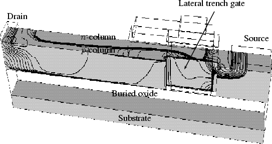 |
Together with the channel on the top of the SOI layer this allows to obtain
an increased channel area compared to that of conventional
SOI-LDMOSFETs. From Figure 4.25 it is clear that only the ![]() -column of
the drift region contributes to the current conduction in the
on-state and the channel current flowing on the side wall of the
trench can be seen. With the increased channel area a reduction of
the channel resistance can be achieved.
-column of
the drift region contributes to the current conduction in the
on-state and the channel current flowing on the side wall of the
trench can be seen. With the increased channel area a reduction of
the channel resistance can be achieved.
An unbalanced structure
which has larger
![]() than
than
![]() is used to examine the
influence of charge imbalance on the on-resistance and the sensitivity
of the BV. Because of the increased
is used to examine the
influence of charge imbalance on the on-resistance and the sensitivity
of the BV. Because of the increased ![]() -column
width
-column
width
![]() from 0.5
from 0.5![]() m (in the case of SJ
SOI-LDMOSFET in Figure 4.24) to 1.0
m (in the case of SJ
SOI-LDMOSFET in Figure 4.24) to 1.0![]() m the doping of this region
is reduced to 6.0
m the doping of this region
is reduced to 6.0 ![]()
![]()
![]() by employing SJ concepts.
by employing SJ concepts.
The width, space, and depth of the lateral trench gate are
0.4![]() m, 1.1
m, 1.1![]() m and 1.0
m and 1.0![]() m, respectively. Simulations
are performed for 120V lateral trench gate SJ SOI-LDMOSFETs
with an
m, respectively. Simulations
are performed for 120V lateral trench gate SJ SOI-LDMOSFETs
with an ![]() -column width
-column width
![]()
![]() 2
2 ![]()
![]() of
1.0
of
1.0![]() m and doping
m and doping
![]() of 6.0
of 6.0 ![]()
![]()
![]() .
The other structure parameters are the same as that in Figure 4.24.
.
The other structure parameters are the same as that in Figure 4.24.