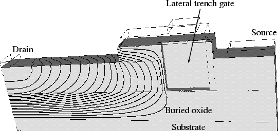
Previous: 4.3.2 Device Structures and Operations Up: 4.3 SJ Lateral Trench Gate SOI-LDMOSFETs Next: 4.4 SJ SOI-LDMOSFETs with Reduced Drift Length
In standard vertical SJ devices the doping of the ![]() - and
- and ![]() -column
of the drift region must be balanced exactly. Most of the previous
works assume that the charge of the
-column
of the drift region must be balanced exactly. Most of the previous
works assume that the charge of the ![]() -column
-column
![]() is equal to that
of the
is equal to that
of the ![]() -column
-column
![]() . The BV depends on the critical electric
field
. The BV depends on the critical electric
field
![]() of the device and the
length of the
of the device and the
length of the ![]() - and
- and ![]() -columns.
-columns.
In the SOI-LDMOSFETs a large portion
of the voltage is supported by the buried oxide layer and
the charge of the ![]() -body affects the RESURF condition significantly.
Unlike in conventional RESURF devices, three-dimensional
RESURF phenomena can be seen in this structure.
-body affects the RESURF condition significantly.
Unlike in conventional RESURF devices, three-dimensional
RESURF phenomena can be seen in this structure.
![]() ,
,
![]() ,
and the charge
,
and the charge
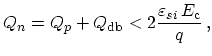
![]() of the p body depletion region should be
balanced. Assuming that all columns are completely depleted before
breakdown, the charges and BV are given by
of the p body depletion region should be
balanced. Assuming that all columns are completely depleted before
breakdown, the charges and BV are given by
 |
(4.1) |
| (4.2) |
| (4.3) |
where
![]() is the length of the
is the length of the ![]() - and
- and ![]() -columns, respectively.
The BV depends both on the critical electric field
-columns, respectively.
The BV depends both on the critical electric field
![]() and the column length.
and the column length.
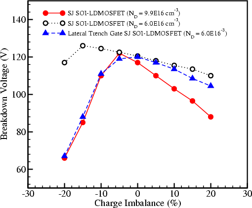
Figure 4.26 shows the ![]() -column doping
-column doping
![]() dependence on the BV
of the SJ SOI-LDMOSFETs, and the doping of the
dependence on the BV
of the SJ SOI-LDMOSFETs, and the doping of the
![]() -column is lower than that of the
-column is lower than that of the ![]() -column.
For the SJ SOI-LDMOSFET with an
-column.
For the SJ SOI-LDMOSFET with an ![]() -column doping
-column doping
![]() of 9.9
of 9.9 ![]()
![]()
![]() , a maximum BV of 124V is obtained
at
, a maximum BV of 124V is obtained
at
![]()
![]() 6.5
6.5 ![]()
![]()
![]() . With the
. With the
![]() of
6.0
of
6.0 ![]()
![]()
![]() , a maximum BV of 127V is
obtained at
, a maximum BV of 127V is
obtained at
![]()
![]() 2.5
2.5 ![]()
![]()
![]() .
These results demonstrate that the charge of the
.
These results demonstrate that the charge of the ![]() -body strongly
affects the charge balance condition of the SJ SOI-LDMOSFETs.
-body strongly
affects the charge balance condition of the SJ SOI-LDMOSFETs.
Figure 4.27 shows the
![]() dependence on the electric field
strength near the surface of the device
along the
dependence on the electric field
strength near the surface of the device
along the ![]() - and
- and ![]() -column junction.
-column junction.
 |
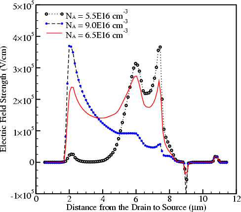 |
At the gate edge a high
electric field can be seen with a low
![]() of 5.5
of 5.5 ![]()
![]()
![]() , and if the
, and if the
![]() is increased
to the value of 9.0
is increased
to the value of 9.0 ![]()
![]()
![]() , a high
electric field is moved toward the drain edge. The optimum electric
field strength distribution is obtained
with the
, a high
electric field is moved toward the drain edge. The optimum electric
field strength distribution is obtained
with the
![]() of 7.0
of 7.0 ![]()
![]()
![]() . It proves that the
optimum RESURF condition can be obtained
with
. It proves that the
optimum RESURF condition can be obtained
with
![]() much lower than
much lower than
![]() .
.
A similar result can be seen for the lateral trench gate SJ
SOI-LDMOSFET (dashed line in Figure 4.26). With an ![]() -column doping
-column doping
![]() of
6.0
of
6.0 ![]()
![]()
![]() and a width
and a width
![]()
![]() 2
2 ![]()
![]() of 1.0
of 1.0![]() m,
the maximum BV is 120V at
m,
the maximum BV is 120V at
![]()
![]() 6.0
6.0 ![]()
![]()
![]() .
Even with a 2 times larger
.
Even with a 2 times larger ![]() -column width than that of the
-column width than that of the ![]() -column
the optimum doping
-column
the optimum doping
![]() is the same as
is the same as
![]() in this case.
in this case.
Figure 4.28 shows the almost uniformly distributed potential lines of a
lateral trench gate SJ SOI-LDMOSFET at the drain voltage
![]() of 120V.
One can clearly see that most of the potential drops over the buried oxide layer.
Curved potential lines at the top surface of the device by
the lateral depletion along the
of 120V.
One can clearly see that most of the potential drops over the buried oxide layer.
Curved potential lines at the top surface of the device by
the lateral depletion along the ![]() - and
- and ![]() -column junction are also visible.
-column junction are also visible.
The BV of SJ devices strongly depends on the charge balance condition.
As has been shown in Figure 4.26, the BV decreases abruptly with decreasing
![]() .
In practical manufacturing it is difficult to achieve perfect charge balance.
Generally, it is assumed that the doping can be controlled within
.
In practical manufacturing it is difficult to achieve perfect charge balance.
Generally, it is assumed that the doping can be controlled within ![]() 10% of the
nominal charge [32].
10% of the
nominal charge [32].
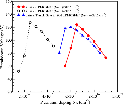
Figure 4.29 shows the sensitivity of the
charge imbalance on the BV. By proper choosing the ![]() -column doping
-column doping
![]() (near the value of the maximum breakdown region in Figure 4.26)
the relations between the BV and the charge imbalance can be seen clearly.
In this figure
(near the value of the maximum breakdown region in Figure 4.26)
the relations between the BV and the charge imbalance can be seen clearly.
In this figure
![]() of 7.0
of 7.0 ![]()
![]()
![]() (SJ SOI-LDMOSFET with
(SJ SOI-LDMOSFET with
![]() of 9.9
of 9.9 ![]()
![]()
![]() ), 3.0
), 3.0 ![]()
![]()
![]() (SJ SOI-LDMOSFET
with
(SJ SOI-LDMOSFET
with
![]() of 6.0
of 6.0 ![]()
![]()
![]() ),
and 6.0
),
and 6.0 ![]()
![]()
![]() (lateral trench gate SJ SOI-LDMOSFET with
(lateral trench gate SJ SOI-LDMOSFET with
![]() of
6.0
of
6.0 ![]()
![]()
![]() ) are used as reference values, respectively.
) are used as reference values, respectively.
As shown in Figure 4.29, this sensitivity (slope of the line) is reduced if the
doping of the drift region is lowered. The drastically reduced sensitivity can be seen
in the SJ SOI-LDMOSFET with a doping concentration
of
![]()
![]() 6.0
6.0 ![]()
![]()
![]() (dotted line).
The reduced BV (110V) with the
(dotted line).
The reduced BV (110V) with the
![]() change from
change from ![]() 20% to
20% to ![]() 20% is
over 90% of the reference value (120V at zero charge imbalance).
20% is
over 90% of the reference value (120V at zero charge imbalance).
 |
However, this results in an increasing on-resistance, which can be overcome
by increasing the ![]() -column width together with the lateral trench gate.
Then it is possible to lower the doping of the drift region without degrading
the on-resistance. The reduced BV (104V) of the lateral trench gate
SJ SOI-LDMOSFET with the
-column width together with the lateral trench gate.
Then it is possible to lower the doping of the drift region without degrading
the on-resistance. The reduced BV (104V) of the lateral trench gate
SJ SOI-LDMOSFET with the
![]() change from 0% to
change from 0% to ![]() 20% is about 87% of
the reference value (120 V). Compared to the BV reduction (88 V) of the
standard SJ SOI-LDMOSFET with
20% is about 87% of
the reference value (120 V). Compared to the BV reduction (88 V) of the
standard SJ SOI-LDMOSFET with
![]() = 9.9
= 9.9 ![]()
![]()
![]() ,
the sensitivity of the BV to the charge imbalance is reduced in the
proposed structure.
,
the sensitivity of the BV to the charge imbalance is reduced in the
proposed structure.
| SJ LDMOSFET on SOI | Lateral trench gate SJ SOI-LDMOSFET | |
|
|
9.9 |
6.0 |
|
|
7.0 |
6.0 |
|
|
2.03m |
1.79m |
| BV | 117V | 120V |
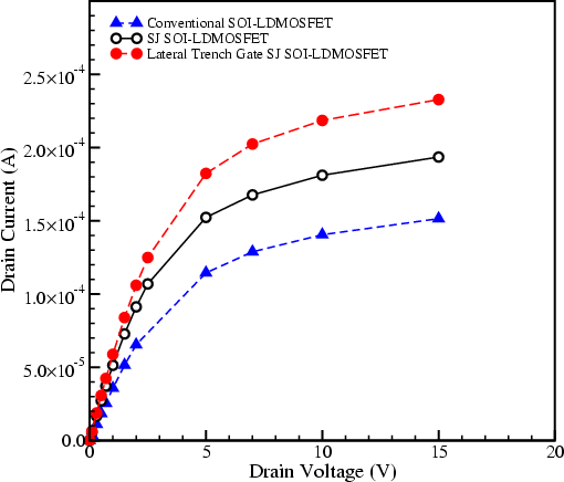
Figure 4.30 and Table 4.3 show the results of the on-state characteristics
of a conventional, a SJ SOI-LDMOSFET, and a lateral trench gate SJ SOI-LDMOSFET.
From this figure it is clear that the lateral trench gate SJ
SOI-LDMOSFET has superior current handling capability compared to the others.
![]() of this device is 1.79m
of this device is 1.79m![]()
![]() at
at
![]()
![]() 12V
and
12V
and
![]()
![]() 0.5V. It is about 60% of the corresponding
0.5V. It is about 60% of the corresponding
![]() value
of a conventional 120V SOI-LDMOSFET (about 3.0m
value
of a conventional 120V SOI-LDMOSFET (about 3.0m![]()
![]() ).
Even the doping of the drift region is reduced by increasing the width
of the
).
Even the doping of the drift region is reduced by increasing the width
of the ![]() -column
-column
![]() is lower than that of the SJ SOI-LDMOSFET with
a much higher
is lower than that of the SJ SOI-LDMOSFET with
a much higher ![]() -column doping up to 9.9
-column doping up to 9.9 ![]()
![]()
![]() .
.
Jong-Mun Park 2004-10-28