
Previous: 4.5.3 Simulation Results Up: 4.5.3 Simulation Results Next: 4.5.3.2 On-State Characteristics
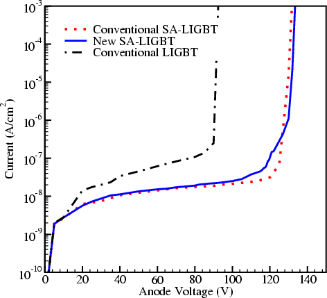
Figure 4.45 shows a comparison of the BV of conventional
SOI-LIGBTs, which have an ![]() -drift length
-drift length
![]()
![]() 8.5
8.5 ![]() m,
and the SOI SA-LIGBT with a trench oxide at the drain/anode.
In the forward blocking state the leakage current of
conventional SOI-LIGBTs depends both on the space charge carrier generation
and the common base current gain of the
m,
and the SOI SA-LIGBT with a trench oxide at the drain/anode.
In the forward blocking state the leakage current of
conventional SOI-LIGBTs depends both on the space charge carrier generation
and the common base current gain of the ![]() -transistor, as a result a
larger leakage current can be seen (dotted-dashed line in Figure 4.45).
As shown in the figure the BV of the SOI SA-LIGBT is higher than that
of the conventional LIGBT. Off-state current gain of the
-transistor, as a result a
larger leakage current can be seen (dotted-dashed line in Figure 4.45).
As shown in the figure the BV of the SOI SA-LIGBT is higher than that
of the conventional LIGBT. Off-state current gain of the ![]() -transistor
affects the blocking voltage of the LIGBT, which is lower compared to
the diode with same drift doping concentration and length. Because the shorted-anode
by the
-transistor
affects the blocking voltage of the LIGBT, which is lower compared to
the diode with same drift doping concentration and length. Because the shorted-anode
by the ![]() -drain effectively reduces the common base current gain of
the
-drain effectively reduces the common base current gain of
the ![]() -transistor(some amount of electrons flow towards the
-transistor(some amount of electrons flow towards the
![]() -drain contact and hole injection from the
-drain contact and hole injection from the ![]() -anode will be suppressed),
SA-LIGBT has a similar high blocking capability to
that of a conventional SOI-LDMOSFET.
-anode will be suppressed),
SA-LIGBT has a similar high blocking capability to
that of a conventional SOI-LDMOSFET.
The conventional SOI-LIGBT has a BV of 90V at
![]()
![]() 8.5
8.5![]() m
and
m
and
![]()
![]() 1.0
1.0 ![]()
![]()
![]() .
The solid line in the figure shows the BV of the proposed SOI SA-LIGBT
with a trench oxide at the drain/anode region. A BV of 130V is obtained with
the same
.
The solid line in the figure shows the BV of the proposed SOI SA-LIGBT
with a trench oxide at the drain/anode region. A BV of 130V is obtained with
the same
![]() as that of the conventional SOI-LIGBT.
Because of the reduced common base current gain of the
as that of the conventional SOI-LIGBT.
Because of the reduced common base current gain of the ![]() -transistor, the BV is much
higher compared to that of the conventional SOI-LIGBT.
As can be seen in the figure it is the same BV as that of the conventional SA-LIGBT.
To prevent a punch through of the depletion layer at the drain/anode,
an
-transistor, the BV is much
higher compared to that of the conventional SOI-LIGBT.
As can be seen in the figure it is the same BV as that of the conventional SA-LIGBT.
To prevent a punch through of the depletion layer at the drain/anode,
an ![]() -buffer layer is added to all the device structures.
Thereby higher forward blocking voltages due to RESURF effect are obtained.
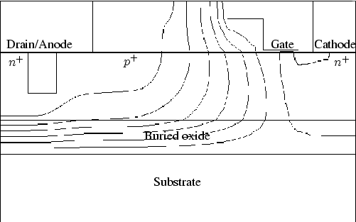
Figure 4.46 shows the potential distribution of the SOI SA-LIGBT
at an anode-cathode voltage
-buffer layer is added to all the device structures.
Thereby higher forward blocking voltages due to RESURF effect are obtained.
Figure 4.46 shows the potential distribution of the SOI SA-LIGBT
at an anode-cathode voltage
![]()
![]() 120V. The potential lines are
suppressed by the highly doped
120V. The potential lines are
suppressed by the highly doped ![]() -buffer and the dense
potential distribution can be seen at the buried oxide layer.
It exhibits a similar potential distribution to that of the conventional SOI
SA-LIGBT, the trench oxide at the drain/anode region does not affect the
RESURF condition.
-buffer and the dense
potential distribution can be seen at the buried oxide layer.
It exhibits a similar potential distribution to that of the conventional SOI
SA-LIGBT, the trench oxide at the drain/anode region does not affect the
RESURF condition.
 |
 |