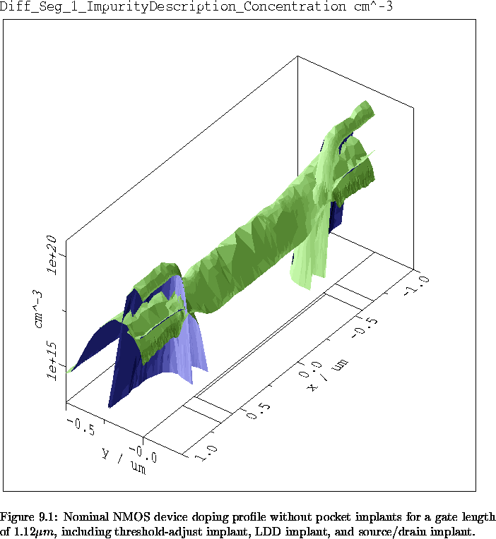
To demonstrate the applicability of the VISTA/SFC simulation
environment to the optimization of the LAT implant parameters,
an NMOS device was designed for a nominal gate length of
![]() and simulated using two-dimensional process and device simulation.
Table 9.2 gives the main process parameters for
the nominal device, Figure 9.5 shows the doping profiles
in the nominal device for the three dopant species boron, arsenic, and
phosphorus.
and simulated using two-dimensional process and device simulation.
Table 9.2 gives the main process parameters for
the nominal device, Figure 9.5 shows the doping profiles
in the nominal device for the three dopant species boron, arsenic, and
phosphorus.
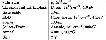
Table 9.2:
Process parameters for NMOS device.