|
|
|
|
Dissertation Christian Poschalko | Previous: 5.1 Calculation of with mode decomposition Up: 5 Introduction of sources and PCB layout structures Next: 5.3 Validation of the trace introduction by HFSS® |
|
|
|
|
Dissertation Christian Poschalko | Previous: 5.1 Calculation of with mode decomposition Up: 5 Introduction of sources and PCB layout structures Next: 5.3 Validation of the trace introduction by HFSS® |
Analytical solutions can be obtained from (4.13) and
(4.14) for rectangular planes. This has been performed for power
integrity analysis by [42] and [43]. This work presents an
analytical solution for a rectangular enclosure in
Chapter 7. Mode decomposition requires numerical
field simulation to extract the partial capacitances in the cross section of transmission
lines on the PCB under the metallic enclosure cover. To enable a purely analytical
solution for efficient design investigations, sources, traces, and planes are introduced
into the cavity field by an analytical distance ratio factor. Complex PCBs usually
consist of numerous traces and planes with different geometric shape, which also requires
numerous simulations in a mode decomposition approach. Therefore, the efficiency of
numerical algorithms for the solution of the cavity field inside enclosures can also be
enhanced significantly by utilization of the proposed analytical introduction method.
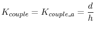
The mode, considered in the cavity model, implies that the field does not vary in
z-dimension. Therefore, the coupling factor
![]() can generally be expressed by a
distance ratio weighting factor
can generally be expressed by a
distance ratio weighting factor
Table 5.1 compares
![]() from (5.9) to
from (5.9) to
![]() from (5.7) for different trace and plane geometries. Values
for
from (5.7) for different trace and plane geometries. Values
for
![]() were obtained by numerical capacitance extraction with the Smart
Analysis Program (SAP) from [75]. A trace thickness of 35
were obtained by numerical capacitance extraction with the Smart
Analysis Program (SAP) from [75]. A trace thickness of 35![]() m was
used in the simulations, because this is often the copper layer thickness of PCBs. The
difference between the two methods for the calculation of the coupling factor
m was
used in the simulations, because this is often the copper layer thickness of PCBs. The
difference between the two methods for the calculation of the coupling factor
![]() is smaller than three percent even for large trace distances to the ground
plane, as in rows 4 and 5. The slight deviation can be explained by the trace thickness,
which is considered in the numerical simulation, but not in (5.9).
On a
is smaller than three percent even for large trace distances to the ground
plane, as in rows 4 and 5. The slight deviation can be explained by the trace thickness,
which is considered in the numerical simulation, but not in (5.9).
On a ![]() scale, usually utilized to compare emission results, a deviation of three
percent equals
scale, usually utilized to compare emission results, a deviation of three
percent equals ![]() . In comparison, the overall emission measurement uncertainty is
usually larger than 3dB, even in very accurate laboratories. This measurement uncertainty
considers, among other uncertainties, the antenna factor uncertainty, the antenna
position tolerance, the site attenuation deviation, and the test receiver tolerances.
Therefore, the accuracy of the analytical factor (5.9) is sufficient
for EMC emission simulations.
. In comparison, the overall emission measurement uncertainty is
usually larger than 3dB, even in very accurate laboratories. This measurement uncertainty
considers, among other uncertainties, the antenna factor uncertainty, the antenna
position tolerance, the site attenuation deviation, and the test receiver tolerances.
Therefore, the accuracy of the analytical factor (5.9) is sufficient
for EMC emission simulations.
C. Poschalko: The Simulation of Emission from Printed Circuit Boards under a Metallic Cover