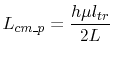
5.7 Link to the current driven common mode mechanism and the common mode inductance
of a trace inside a cavity.
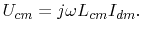
The magnetic flux lines wrapping around the ground plane of a PCB cause a voltage between
wires which are connected at the PCB [32].
Figure 5.14 shows the magnetic flux and the associated common
mode voltage  , which drives the cables, connected to the PCB like an antenna
source voltage.
, which drives the cables, connected to the PCB like an antenna
source voltage.
Figure 5.14:
Model illustrating the physics of the current driven common mode mechanism as
described in [32].
|
![\includegraphics[height=5.4 cm,viewport=60 570 520 750,clip]{pics/CM_Cable.eps}](img413.png) |
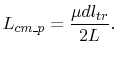
The differential mode current on the trace  and common mode inductance
  determine the common mode voltage
 |
(5.18) |
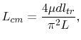
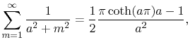
For a trace in the symmetry line (x=L/2) of the ground plane (Trace a in
Figure 5.15) the common mode inductance is
 |
(5.19) |
according to [36]. The trace length is  .
.
Figure 5.15:
Trace a in the symmetry line of the ground plane and Trace b located at a
distance s from that symmetry line.
|
![\includegraphics[height=3.3 cm,viewport=140 630 450
740,clip]{pics/CM_Cable_middle.eps}](img417.png) |
The trace inductance for a trace located at a distance s from the ground plane symmetry
line (Trace b in Figure 5.15) is
 |
(5.20) |
according to [37]. For a trace in the symmetry line of the ground plane (s=0)
[37] reduced (5.20) to
 |
(5.21) |
The equations (5.19) and (5.21) have
been obtained for a narrow trace
 above the PCB ground plane and without a
metallic cover plane. For a parallel plane structure
above the PCB ground plane and without a
metallic cover plane. For a parallel plane structure  , trace width = ground
plane width) the common mode inductance is
, trace width = ground
plane width) the common mode inductance is
 |
(5.22) |
according to [36], where h is the plane separation distance.
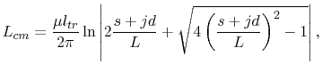
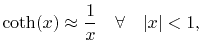
A  -TEM cell measurement and a hybrid coupler was carried out by [99] for
the coupling from heat sinks to cables and by [100] for the magnetic field
coupling to cables. This measurement configuration is shown in
Figure 5.16. The coordinate system definition is consistent with
those in Figure 5.14 and
Figure 5.15.
-TEM cell measurement and a hybrid coupler was carried out by [99] for
the coupling from heat sinks to cables and by [100] for the magnetic field
coupling to cables. This measurement configuration is shown in
Figure 5.16. The coordinate system definition is consistent with
those in Figure 5.14 and
Figure 5.15.
Figure 5.16:
Measurement configuration of [100] to obtain the magnetic coupling
moment of a trace or an IC.
|
![\includegraphics[height=8.6 cm,viewport=90 510 480 770,clip]{pics/TEMCell.eps}](img423.png) |
The magnetic field coupling moment is obtained from the  output of the hybrid
coupler by [100].
output of the hybrid
coupler by [100].
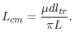
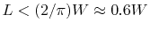
To obtain the magnetic coupling of a trace to the cavity
between two parallel rectangular planes, the model depicted in
Figure 5.17 is utilized.
Figure 5.17:
Model for the derivation of the coupling inductance from a trace to the
cavity.
|
![\includegraphics[height=6.5 cm,viewport=130 570 480
760,clip]{pics/Open_Edges_TEM.eps}](img425.png) |
Neglecting the  terms in (4.19) and (4.20) and inserting
these equations into (4.18) yields
terms in (4.19) and (4.20) and inserting
these equations into (4.18) yields
![$\displaystyle Z_{ij}=\frac{j\omega\mu
h}{LW}\sum_{m=0}^{\infty}\sum_{n=0}^{\in...
...(k_{n}y_{i})
\cos(k_{m}x_{j})\cos(k_{n}y_{j})}{{k_{m}^2+k_{n}^2-k^2}} \right],$](img427.png) |
(5.23) |
for the mutual impedance between two parallel-plane ports.
With the ports and sources in Figure 5.17 the voltage difference of
port A and B becomes
![$\displaystyle M_{c}=
\frac{8\mu d}{LW}
\sum_{n=0}^{\infty}\left\{(-1)^n
\sin...
...\infty}
\frac{2}{(\frac{2m\pi}{L})^2+(\frac{(2n+1)\pi}{W})^2} \right]\right\}.$](img428.png) |
(5.24) |
where  is the wavelength. The factors
  are one for
  and two for
nonzero m.
The factors
and two for
nonzero m.
The factors  are one for
  and two for nonzero n. The factor
  considers
the trace coupling according to Section 5.2. According to the factor
considers
the trace coupling according to Section 5.2. According to the factor
 terms with even
  vanish. For low frequencies
 the nominator term
 may be neglected. With this simplification, (5.24) becomes
![$\displaystyle M_{c}=
\frac{8\mu d}{LW}
\sum_{n=0}^{\infty}\left\{(-1)^n
\sin...
...\infty}
\frac{2}{(\frac{2m\pi}{L})^2+(\frac{(2n+1)\pi}{W})^2} \right]\right\}.$](img438.png) |
(5.25) |
The coupling inductance is
![$\displaystyle M_{c}=
\frac{8\mu d}{LW}
\sum_{n=0}^{\infty}\left\{(-1)^n
\sin...
...\infty}
\frac{2}{(\frac{2m\pi}{L})^2+(\frac{(2n+1)\pi}{W})^2} \right]\right\}.$](img439.png) |
(5.26) |
With
 |
(5.27) |
(5.26) is simplified to
![$\displaystyle M_{c}=
\frac{4\mu d}{\pi}\sum_{n=0}^{\infty}\left[(-1)^n \sin\le...
...l_{tr}}{2W}\right)\frac{\coth\left(\frac{(2n+1)\pi L}{2W}\right)}{2n+1}\right].$](img441.png) |
(5.28) |
For small traces
 the function described by the fourier series in
(5.28) is approximated by the first term of its Taylor series,
developed
around
the function described by the fourier series in
(5.28) is approximated by the first term of its Taylor series,
developed
around  and (5.28) becomes
![$\displaystyle M_{c}=
\frac{2\mu dl_{tr}}{W}\sum_{n=0}^{\infty}\left[(-1)^n\coth\left(\frac{(2n+1)\pi
L}{2W}\right)\right].$](img444.png) |
(5.29) |
With
![$\displaystyle \sum_{n=0}^{\infty}\left[(-1)^n\coth\left(\frac{(2n+1)\pi L}{2W}\right)\right]\approx
\frac{\pi}{4}\coth\left(\frac{L\pi}{2W}\right)$](img445.png) |
(5.30) |
and
 |
(5.31) |
the coupling inductance for
 becomes
 |
(5.32) |
The common mode inductance is associated with the flux wrapping around only one of the
two planes. Thus, the coupling inductance has to be divided by a factor of two to obtain
the common mode inductance [36]. Therefore, the common mode inductance of
a trace inside a
parallel plane cavity is
 |
(5.33) |
Note that (5.33) becomes exactly
(5.22)
of [36], when the trace height above the ground plane becomes the plane
separation distance  . Equation (5.22) has been verified
experimentally by
[36]. This provides evidence that the current driven common mode
coupling mechanism of a trace inside a parallel-plane cavity is described sufficiently
with the
cavity model. The cavity model describes not only the current driven common mode
mechanism for
a tiny trace in the symmetry line of the cavity, but also the current driven common mode
coupling for arbitrary traces inside the cavity.
. Equation (5.22) has been verified
experimentally by
[36]. This provides evidence that the current driven common mode
coupling mechanism of a trace inside a parallel-plane cavity is described sufficiently
with the
cavity model. The cavity model describes not only the current driven common mode
mechanism for
a tiny trace in the symmetry line of the cavity, but also the current driven common mode
coupling for arbitrary traces inside the cavity.
The verification of the common mode inductance by measurement has been carried out as
follows. Figure 5.18(a) shows the measurement setup with the VNA
(vector network analyzer) ZVB4 from Rhode&Schwarz. A trace loop above a copper plane is
connected to one port of the VNA. The trace is terminated with 0 Ohm to the ground copper
plane. A wire loop is soldered to both ends of the copper plane and a SMA connector in
this loop is connected to the second VNA port for the measurement of the induced common
mode loop voltage. This is illustrated in Figure 5.18(b) and
Figure 5.18(c). The measured S parameters are converted to Z
parameters and the common mode inductance
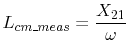 ,with ,with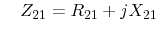 |
(5.34) |
is calculated from the measurement results. The measurement is carried out for a trace
above ground without a cover plane in Figure 5.18(b) and for a
configuration with a cover plane at a distance of 10mm from the ground plane as depicted
in Figure 5.18(d). The cover plane was tightly arranged with foam
plates with a dielectric constant close to that of air and an adhesive tape. The
dimensions for the test device are listed in Table 5.4.
Figure 5.18(e) shows good agreement of the measured common mode
inductances to the analytical results from (5.21) of 0.08nH
for the configuration without a cover plane and to the result from
(5.33) of 0.12nH for the configuration with a cover plane. This
confirms that the current driven common mode coupling is sufficiently described with the
cavity model.
![\includegraphics[height=5 cm]{CM_Measure_1.eps}](img452.png)
![\includegraphics[height=5 cm,viewport=30 40 835
545,clip, clip]{CM_Measure_2.eps}](img453.png)
| (a) Measurement setup overview. | (b) Trace loop above ground. |
|
![\includegraphics[height=5 cm]{CM_Measure_3.eps}](img454.png)
![\includegraphics[height=5 cm,viewport=30 40 835
545,clip, clip]{CM_Measure_4.eps}](img455.png)
| (c) Induced voltage measurement loop. | (d) Trace inside a cavity. |
|
|
![\includegraphics[height=6 cm,viewport=180 295 420
485,clip]{pics/CM_Ind_Result.eps}](img456.png)
| (d) Measured common mode inductances. |
|
Figure 5.18:
Measurement setup and results for the validation of the common mode
inductance.
| Designation |
Dimension |
|
 |
120 |
mm |
 |
50 |
mm |
|
10 |
mm |
 |
1 |
mm |
|
10 |
mm |
 |
2 |
mm |
|
Table 5.4:
Dimensions of the test device.
C. Poschalko: The Simulation of Emission from Printed Circuit Boards under a Metallic Cover