7.3 Comparison of the analytical model results to HFSS®
simulations and measurement results
For the validation of the analytical models of Section 7.1
and Section 7.2, results for the electric far field
density from an enclosure with dimensions depicted in
Figure 7.4 are obtained with the analytical models,
with three-dimensional full wave simulation, and with measurements.
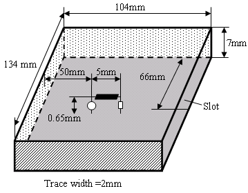
Figure 7.4:
Enclosure dimensions and source position for the validation of the analytical
model results for the electric far field.
The geometric dimensions are practically relevant, because they are similar to those of
the parallel plane cavity between the PCB ground plane and the enclosure bottom of a
typical automotive control device depicted in Figure 1.1(a). However, there
are geometrical deviations between the shape of an automotive control device enclosure
and a rectangular enclosure. Therefore, the validation of the analytical model is carried
out on a rectangular test enclosure. The test enclosure in
Figure 7.5 is manufactured from copper sheets which are
soldered together at the edges. Thus, the geometry dimensions of the test enclosure match
the simulation models. The comparison is carried out for 0 W, 50 W, and
1e9 W (open in the measurement). A removable SMA connector with a short copper
trace soldered to the rigid SMA wire was used to enable the change of the trace loads.
Figure 7.5(a) depicts the test enclosure with mounted SMA
connector.
![\includegraphics[height=4.5 cm,viewport=80 130 510
400,clip]{pics/Enc_Cu_Measure.eps}](img572.png)
![\includegraphics[height=4.5 cm,viewport=80 470 510
740,clip]{pics/Measure_1.eps}](img573.png)
| (a) Enclosure with removable SMA connector. | (b) SMA connector with test trace removed. |
Figure 7.5:
Copper test enclosure for the validation with measurements.
To obtain a reasonably good contact of the SMA connector ground to the enclosure, a
conducting silver painting and conducting copper tapes were used to mount the connector.
Before mounting the connector, the copper plane surface was cleaned accurately and the
surface oxide was removed. Figure 7.5(b) shows the test
enclosure with removed SMA connector. The measurements have been carried out with a horn
antenna (Amplifier Research [107] AT4002A in
Figure 7.6(d)) and a vector network analyzer (Rhode &
Schwarz ZVB4) inside a semi-anechoic chamber. Pyramid absorbers have been added on the
bottom of the chamber, between the measurement antenna and the test device to obtain
similar conditions to those in a fully anechoic chamber. These absorbers can be seen in
Figure 7.6(a). The electric field was calculated and measured
1m in front of the enclosure slot. This position has been selected as the main lob of the
electric field distribution is oriented in this direction for some of the resonance
frequencies within the evaluated frequency range of 800 MHz to 4 GHz. The position is
consistent with CISPR 25 Edition 3 [56] for automotive component emission
measurements above 1 GHz. A measurement setup overview is depicted in
Figure 7.6(c) and the connection of the network analyzer
cable to the enclosure SMA connector is depicted in
Figure 7.6(b).
![\includegraphics[height=4.5 cm,viewport=80 130 510
400,clip]{pics/Measure_1.eps}](img574.png)
![\includegraphics[height=4.5 cm,viewport=80 130 510
400,clip]{pics/Measure_1.eps}](img575.png)
| (a) Bottom absorbers for anechoic conditions. | (b) Connection of the enclosure. |
![\includegraphics[height=4.5 cm,viewport=80 130 510
400,clip]{pics/Measure_2.eps}](img576.png)
![\includegraphics[height=4.5 cm,viewport=80 130 510
400,clip]{pics/Measure_2.eps}](img577.png)
| (c) Measurement setup overview. | (d) Antenna (Amplifier Research AT4002A). |
Figure 7.6:
Setup for the validation measurement with a horn antenna from 800MHz to 4GHz.
Table 7.2 contains a summary of the measurement equipment.
Table 7.2:
Measurement equipment.
| Equipment |
Designation |
Supplier |
|
| Horn antenna |
AT4002A |
Amplifier Research |
[107] |
| Network analyzer |
ZVB4 |
Rhode & Schwarz |
[108] |
| Calibration set |
R&S®ZV-Z21 |
Rhode & Schwarz |
[108] |
| Ferrite Sleeve |
7427114 |
Würth Elektronik |
[109] |
| Ferrite Sleeve |
7427733 |
Würth Elektronik |
[109] |
|
Ferrite sleeves have been arranged on the coaxial cables, close to the connectors, to
suppress currents on the cable shield. The ferrite sleeve, 7427114 from Würth Elektronik
[109], applied close to the SMA connector of the enclosure provides an impedance
of about 200 W at about 1 GHz. A second sleeve 7427733 was applied on the antenna
cable. The network analyzer was calibrated with a two port TOSM calibration using the
calibration set R&S®ZV-Z21 from Rhode & Schwarz [108]. The measurement bandwidth
was 10Hz for maximum noise suppression.
The comparison of the cavity model results, the HFSS® simulation
results, and the measurement results depicted in Figure 7.8
shows a reasonably good agreement. This confirms the analytical models of
Section 7.1 and Section 7.2.
The utilized equation (7.32) for the electric far
field considers only the radiation from the enclosure slot and neglects the metallic
enclosure walls that have some influence on the radiation diagram above the first
resonance frequency. However, this is a reasonable simplification, also applied to obtain
basic radiation characteristics of horn antennas [104].
Therefore, (7.32) can be used to obtain a good first
order information about the radiated field. Figure 7.8 shows
not only slight deviations between the measurement results and the cavity model results.
It also shows some deviations of the measurement results from the results of the
three-dimensional full wave simulation with HFSS®, which considers the
influence of the enclosure walls. Thus, the comparison deviations in
Figure 7.8 can be explained mainly from the test enclosure
tolerances and test site uncertainties. However, there are maximal 3dB magnitude
deviations between the maxima of the cavity model results and the measurements.
The consideration of the radiation loss for the calculation of the slot voltages is
crucial to obtain the correct voltage distribution inside the enclosure and the correct
radiated far field. Figure 7.7 shows a comparison
between the electric far-field obtained from a cavity field model which considers the
radiation loss and a cavity model which neglects the radiation loss. For practical
simulation investigations an EMC engineer needs quantitative information about the
electric far field magnitude, especially at the resonances at which the radiation is at
its maximum. A model that neglects the radiation loss with deviations at the resonances
of more than 30dB is not sufficient for EMC simulation purposes.
![\includegraphics[height=7 cm,viewport=90 295 520
485,clip]{pics/Val_Horn_Enc_0.eps}](img579.png)
Figure 7.7:
Electric far field, one meter in front of the enclosure slot. Comparison of the
cavity model results, which includes the radiation loss by introducing the admittance
matrix
 , into the results obtained from a cavity field which does not
consider the radiation loss.
, into the results obtained from a cavity field which does not
consider the radiation loss.
![\includegraphics[height=3 cm,viewport=115 205 505 600,clip]{pics/Rad1.eps}](img580.png)
![\includegraphics[height=3 cm,viewport=115 205 505 600,clip]{pics/Rad1.eps}](img581.png)
![\includegraphics[height=3 cm,viewport=115 205 505 600,clip]{pics/Rad1.eps}](img582.png)
Figure 7.8:
Electric far-field 1m in front of the enclosure slot. Comparison of the cavity
model results with the HFSS® simulation results and measurement
results.
C. Poschalko: The Simulation of Emission from Printed Circuit Boards under a Metallic Cover