next up previous
Next: 3.2.3.2 Band Gap Offsets Up: 3.2.3 Band Structure Parameters Previous: 3.2.3 Band Structure Parameters

3.2.3.1 The Band Gap

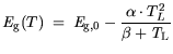
The band gap is the most important parameter for the description of semiconductors. It is modeled as a function of lattice temperature according to:

    $\displaystyle {\it E}_\mathrm{g}(T) = {\it E}_\mathrm{g,0}- \frac{\alpha \cdot T^2_L}{\beta + {\it T}_\mathrm{L}}$ (3.21)

where $ {\it E}_\mathrm{g,0}$ is the extrapolated band gap at $ {\it T}_\mathrm{L}$= 0 K. The parameter values and values at $ {\it T}_\mathrm{L}$= 300 K are given in Table 3.5.

Table 3.5: Band gap parameters for elementary and binary semiconductors.
Material Minimum $ {\it E}_\mathrm{g,0}$ $ \alpha$ $ \beta$ ReFported Range Rep.Range References
    [eV] [eV/K] [K] $ {\it E}_\mathrm{g,0}$ [eV] $ {\it E}_\mathrm{g,300}$ [eV]  
GaAs $ \Gamma$ 1.521 5.58 $ \cdot 10^{-4}$ 220 1.517-1.55 1.424 [284,222]
AlAs X 2.239 6.0 $ \cdot 10^{-4}$ 408 2.22-2.239 2.14, 2.163, 2.168 [91,265,110]
InAs $ \Gamma$ 0.420 2.5 $ \cdot 10^{-4}$ 75 0.414-0.43 0.36 [284]
  also 0.43 2.76-3.16 $ \cdot 10^{-4}$ 83-93 0.42-0.43   [315]
InP $ \Gamma$ 1.421 3.63 $ \cdot 10^{-4}$ 162 1.42-1.432 1.35 [284]
GaN $ \Gamma^{dir}$ 3.50 7.32 $ \cdot 10^{-4}$ 700 3.51 3.2, 3.39,3.43 [224,280,303]
AlN $ \Gamma^{indir}$ 6.312 1.7999 $ \cdot
10^{-3}$ 1462 6.118 6.02-6.2 [224,255]
InN $ \Gamma$ 2.01 1.2 $ \cdot
10^{-3}$ 627 2.00 1.89-1.95 [206,291]
Si X 1.1695 4.73 $ \cdot 10^{-4}$ 636 1.17 1.124 [194,265,284]


The significant scatter for the values of nitride based semiconductors is due to the high unintentional background concentrations, for InN $ {\it N}_{\mathrm{D}}>$ 10$ ^{19}$ cm$ ^{-3}$. For the ternary semiconductors the band gap is modeled following a k-valley dependent approach. For HEMTs used in this work the material compositions are sometimes close to the cross over transition in k-space, e.g. for Al$ _x$Ga$ _{1-x}$As at $ x$= 0.45, or for In$ _x$Al$ _{1-x}$As at $ x$= 0.3. To achieve a better modeling, instead of using a simple bowing over the cross-over transition, two sets of parameters are given.

Table 3.6: Additional band gap parameters for binary semiconductors.
Material Minimum $ {\it E}_\mathrm{g,0}$ $ \alpha$ $ \beta$ Rep. Range Rep. $ {\it E}_\mathrm{g,300}$ References
    [eV] [eV/K] [K] $ {\it E}_\mathrm{g,0}$ [eV] [eV]  
GaAs $ X$ 1.981 4.6 $ \cdot 10^{-4}$ 204 - 1.899 -1.91 [2,213]
              [264]
AlAs $ \Gamma$ 2.891 8.78 $ \cdot 10^{-4}$ 332 2.907-3.02 2.95 [2,152]
              [213,263]
InAs $ X$ 2.278 5.78 $ \cdot 10^{-4}$ 83 - 2.142 [152,257]
InP $ X$ 2.32 7.66 $ \cdot 10^{-4}$ 327 2.32-2.38 2.21 [4]
AlN $ \Gamma^{dir}$ 7.0 1.7999 $ \cdot
10^{-3}$ (1462) - 6.9 [96]


Table 3.6 introduces this two-valley modeling, which includes independent values e.g. for X-valley AlAs and $ \Gamma$-valley AlAs for the different minimum valleys. These values are only used for those material compositions, where they are physically relevant, i.e., $ \Gamma$-AlAs only for Al$ _x$Ga$ _{1-x}$As with $ x$$ \leq$ 0.45, while for $ x$$ \geq$ 0.45, the value of X-AlAs is chosen. The split into two different parameter sets allows for a more precise modeling than the conventional one valley bowing approach, as shown in the following. The band gap of an alloy A$ _x$B$ _{1-x}$ is calculated as:
    $\displaystyle E_{g,i}^{AB} = x \cdot E_{g,A} + (1-x) \cdot E_{g,B} + x \cdot (1-x) \cdot C_{g,i}$ (3.22)

where i stands for either $ \Gamma$ or $ X$. The valid band gap is used according to:
    $\displaystyle E_{g,i}^{AB} = $min$\displaystyle \big(E_{g \Gamma}^{AB}, E_{g X}^{AB} \big)$ (3.23)

The parameters for both valleys are given in Table 3.6. As was also shown in [207] also the conventional approach neglecting the cross over transition is presented in Table 3.7 and (3.25).
    $\displaystyle E_{g}^{AB}  = x \cdot E_{g,A} + (1-x) \cdot E_{g,B} + x \cdot (1-x) \cdot C_{g}$ (3.24)


Table 3.7: Band gap parameters for ternary semiconductors.
Material $ C_{g,\Gamma}$ $ C_{g,X}$ $ C_{g one valley}$ Reported Range References
  [eV] [eV] [eV] [eV]  
Al$ _{x}$Ga$ _{1-x}$As 0 -0.143 0.7 - [222,250]
In$ _{x}$Ga$ _{1-x}$As - - -0.475 - [265,315]
In$ _{x}$Al$ _{1-x}$As -0.3 -0.713 1.2 1.45 ($ x$=0.52) [163]
Al$ _{x}$Ga$ _{1-x}$N -1.65 (first valley) - -1.2596 3.88 ($ x$=0.2) [255,303]
In$ _{x}$Ga$ _{1-x}$N -2.05 - -2.05 - [303]


Figure 3.2: Bowing parameters for the band gap in

Al$_x$Ga$_{1-x}$N [255,303].

\includegraphics[width=10 cm]{D:/Userquay/Promotion/HtmlDiss/fig3b.eps}

The significant scatter for the bowing parameter in AlGaN was resolved in [303] for $ x$$ <$ 0.16 and is attributed to a systematic discrepancy of the two experimental methods applied. From this data a specific $ \Gamma$ (first)-valley value for the bowing parameter was obtained. Data from [255] were evaluated in a one valley model for a consistent description of the cross over transition, as shown in Fig. 3.2. For In$ _x$Ga$ _{1-x}$N, as a first approach, the strained data were compiled into the model for $ x$$ <$ 0.15.


next up previous
Next: 3.2.3.2 Band Gap Offsets Up: 3.2.3 Band Structure Parameters Previous: 3.2.3 Band Structure Parameters
Quay
2001-12-21