


Next: 4.1.1.4 Contributions to the
Up: 4.1.1 The Basic Model
Previous: 4.1.1.2 Contributions to
The drain source capacitance
 originates from the capacitive coupling of the
source and drain and represents the intrinsic output capacitance in the standard model of
Fig. 4.1. Bias dependent contributions to
arise from buffer and channel layers
depending on the channel carrier distribution. Since a one-dimensional model does not consider a
originates from the capacitive coupling of the
source and drain and represents the intrinsic output capacitance in the standard model of
Fig. 4.1. Bias dependent contributions to
arise from buffer and channel layers
depending on the channel carrier distribution. Since a one-dimensional model does not consider a
 voltage, the analysis remains for a two- or three-dimensional model.
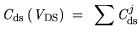
can be
written as:
voltage, the analysis remains for a two- or three-dimensional model.
can be
written as:
| |
|
 |
(4.6) |
where the index j represents all layers between gate metal and semi-insulating substrate
in Fig. 3.1.
Thus, the elements
 ,
,
 ,
,
 , and even
find a relatively neat physical interpretation in compact
models. For the other four elements a physical interpretation can
be found, but unfortunately the non-ambiguous transformation of
eight S-parameters into eight small-signal elements leads to
rather abstract quantities for their physical interpretation.
, and even
find a relatively neat physical interpretation in compact
models. For the other four elements a physical interpretation can
be found, but unfortunately the non-ambiguous transformation of
eight S-parameters into eight small-signal elements leads to
rather abstract quantities for their physical interpretation.
Quay
2001-12-21