« PreviousUpNext »Contents
Previous: 1 Introduction Top: 1 Introduction Next: 1.3 Methodology
1.2 Detrimental Effects in MOS Devices
Despite all the advantages of SiC, commercially available devices perform far from their theoretical limits. This is mainly due to the fact that the larger band gap of  at
300 K leads to extended interactions of free carriers with interfacial trap states. The energetic positions of these states are within the SiC band gap but outside the silicon band gap and lead to enlarged hysteresis effects
[24–29], which are investigated in Chapter 2, and bias temperature instability (BTI), as will be discussed in Chapter 3. Although there have been enormous improvements to the electrical performance within the last years by interface annealing in nitrogen
containing atmospheres, like nitrous oxide (N2O) or nitric oxide (NO), SiC-based power MOSFETs still show one to two orders of magnitude higher interface state densities
at
300 K leads to extended interactions of free carriers with interfacial trap states. The energetic positions of these states are within the SiC band gap but outside the silicon band gap and lead to enlarged hysteresis effects
[24–29], which are investigated in Chapter 2, and bias temperature instability (BTI), as will be discussed in Chapter 3. Although there have been enormous improvements to the electrical performance within the last years by interface annealing in nitrogen
containing atmospheres, like nitrous oxide (N2O) or nitric oxide (NO), SiC-based power MOSFETs still show one to two orders of magnitude higher interface state densities  as their silicon based counterparts [30–35].
1.2.1 Bias Temperature Instability
Bias temperature instability (BTI), as one of the main topics of interest in countless reliability studies based on 4H-SiC MOSFETs [36–44], is caused by charge trapping at or near the SiC/SiO2 interface during (high
temperature) gate stress, resulting in threshold voltage  variations, which depend on the polarity of the
stress voltage. A positive gate stress results in electron capture leading to shifts to more positive gate voltages, whereas a
negative gate stress shifts to more negative gate voltages. Especially for
SiC based power devices, a large positive voltage shift
variations, which depend on the polarity of the
stress voltage. A positive gate stress results in electron capture leading to shifts to more positive gate voltages, whereas a
negative gate stress shifts to more negative gate voltages. Especially for
SiC based power devices, a large positive voltage shift  is undesirable because the voltage overdrive in the on-state is decreased. This is
mainly a problem because unlike in silicon based power devices, the contribution of the channel resistance
is undesirable because the voltage overdrive in the on-state is decreased. This is
mainly a problem because unlike in silicon based power devices, the contribution of the channel resistance  to the total on-resistance
  is significantly higher in SiC devices. Here,
accounts for up to 50 % of the total
. Therefore, a reduction of the overdrive leads to
a significant increase in the on-resistance and static losses, respectively. A more detailed
discussion on the application relevance of BTI for SiC-MOSFETs is given in [43].
is significantly higher in SiC devices. Here,
accounts for up to 50 % of the total
. Therefore, a reduction of the overdrive leads to
a significant increase in the on-resistance and static losses, respectively. A more detailed
discussion on the application relevance of BTI for SiC-MOSFETs is given in [43].
Theoretical background
BTI results from charge trapping at or near the semiconductor-insulator interface after the creation of new defects from precursors or charging of preexisting defects [45, 46]. Despite the fact that BTI in silicon based devices has
been investigated for more than half a century, the detailed atomic origin is still heavily debated. Several microscopic defect candidates are under intensive investigation, including various interactions with hydrogen (diffusion,
hopping, depassivation of silicon dangling bonds etc.) [47, 48], SiO2 intrinsic electron traps [49, 50], oxygen vacancies [51, 52] or dangling bonds [53, 54]. Although the absolute is more pronounced in SiC based devices, likely due to the larger band-gap, the
BTI characteristics are, at least to some extent, analogous to Si based devices, indicating similar atomic origins. In Section 1.2.2, a more detailed overview
on a hydrogen (H) related model (the H release model) is provided, which tries to link the permanent BTI component with H released from the gate-side of the MOSFET and is able to explain many features of BTI.
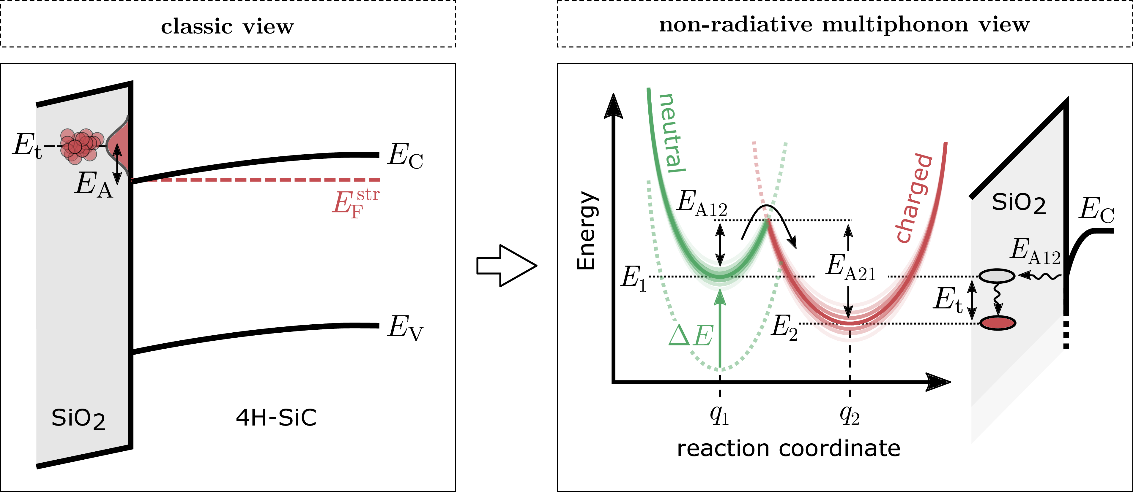
Figure 1.6: Left: classic view of the trapping mechanism extended with a distributed trap level which results in a distributed activation energy  . Right: modern interpretation using non-radiative
multiphonon (NMP) theory with distributed activation energies for capture (12) and emission (21) processes.
. Right: modern interpretation using non-radiative
multiphonon (NMP) theory with distributed activation energies for capture (12) and emission (21) processes.
A often used model for the charge trapping mechanism is shown in Fig. 1.6 (left) assuming a single trap state at the energy level  within the oxide close to the
SiC/SiO2 interface. At a fixed Fermi-level (e.g during constant bias stress) the classic model is extended by introducing an activation energy . Furthermore, the activation energy of the trap
state to change its occupancy is assumed to be normally distributed. A more comprehensive explanation of the atomic mechanism is given by the NMP model (Fig. 1.6, right), which also accounts for the atomic deformation of the defect when the charge state is changed and the electric field dependency for both, capture
and emission times of the defect [55, 56]. In the NMP model the neutral and charged state of a defect are described as a parabolic function representing the possible energy states (cf. quantum harmonic oscillator) as depicted in Fig.
1.6 (right). Here
within the oxide close to the
SiC/SiO2 interface. At a fixed Fermi-level (e.g during constant bias stress) the classic model is extended by introducing an activation energy . Furthermore, the activation energy of the trap
state to change its occupancy is assumed to be normally distributed. A more comprehensive explanation of the atomic mechanism is given by the NMP model (Fig. 1.6, right), which also accounts for the atomic deformation of the defect when the charge state is changed and the electric field dependency for both, capture
and emission times of the defect [55, 56]. In the NMP model the neutral and charged state of a defect are described as a parabolic function representing the possible energy states (cf. quantum harmonic oscillator) as depicted in Fig.
1.6 (right). Here  and
and  are the reaction coordinate equilibrium positions
with the distributed local ground state energies
are the reaction coordinate equilibrium positions
with the distributed local ground state energies  and
and  of the neutral and charged state, respectively.
The required activation energy for a transition of the charge state depends on the ground state energy and the shape of the energy potentials (parabolas). As an example, we start with a neutral precursor described by the green
parabola. After providing enough energy 12 through lattice vibrations to
change the charge state, the state configuration changes (e.g bond length, equilibrium nuclei position etc.) and is now described by the red parabola. Hence, the activation energy for the reverse transition from the charged (red) to
the neutral (green) state is given by 21, which usually differs from 12.
Assuming a distributed , the capture/emission process is distributed in
time according to the characteristic capture or emission time constant 

with the Boltzmann constant  , the temperature
  and the pre-exponential factor
  .
.
The influence of distributed activation energies on the observed voltage shift during stress and recovery is shown in Fig. 1.7. For instance, a normally distributed with a mean value  and standard deviation
 (green, top) will lead to a voltage shift versus
stress time behavior with trapping times within 1 × 10⁴ s and 1 × 10¹² s (middle, green). Increasing the width of the distribution will lead to a larger stretch out of
the stress time dependence as shown in blue (,
(green, top) will lead to a voltage shift versus
stress time behavior with trapping times within 1 × 10⁴ s and 1 × 10¹² s (middle, green). Increasing the width of the distribution will lead to a larger stretch out of
the stress time dependence as shown in blue (,  ) and red (
 ,
,  ). The bottom picture in Fig. 1.7 represents the discharging behavior for the same set of activation energies assuming all trapping centers have been filled during the preceding stress. In
real devices, a combination of various defects with characteristic energy barriers will contribute, leading to a convolution of the individual voltage shift vs time behaviors [46]. For broadly distributed activation energies, approaches the often used power-law approximation
). The bottom picture in Fig. 1.7 represents the discharging behavior for the same set of activation energies assuming all trapping centers have been filled during the preceding stress. In
real devices, a combination of various defects with characteristic energy barriers will contribute, leading to a convolution of the individual voltage shift vs time behaviors [46]. For broadly distributed activation energies, approaches the often used power-law approximation

with the pre-factor  and the power-law factor
  , which is only valid within a narrow time window. An example of a mixture between
two individual defects (red and blue) is given in Fig. 1.7 as a dashed black line for stress (middle) and recovery (bottom).
, which is only valid within a narrow time window. An example of a mixture between
two individual defects (red and blue) is given in Fig. 1.7 as a dashed black line for stress (middle) and recovery (bottom).
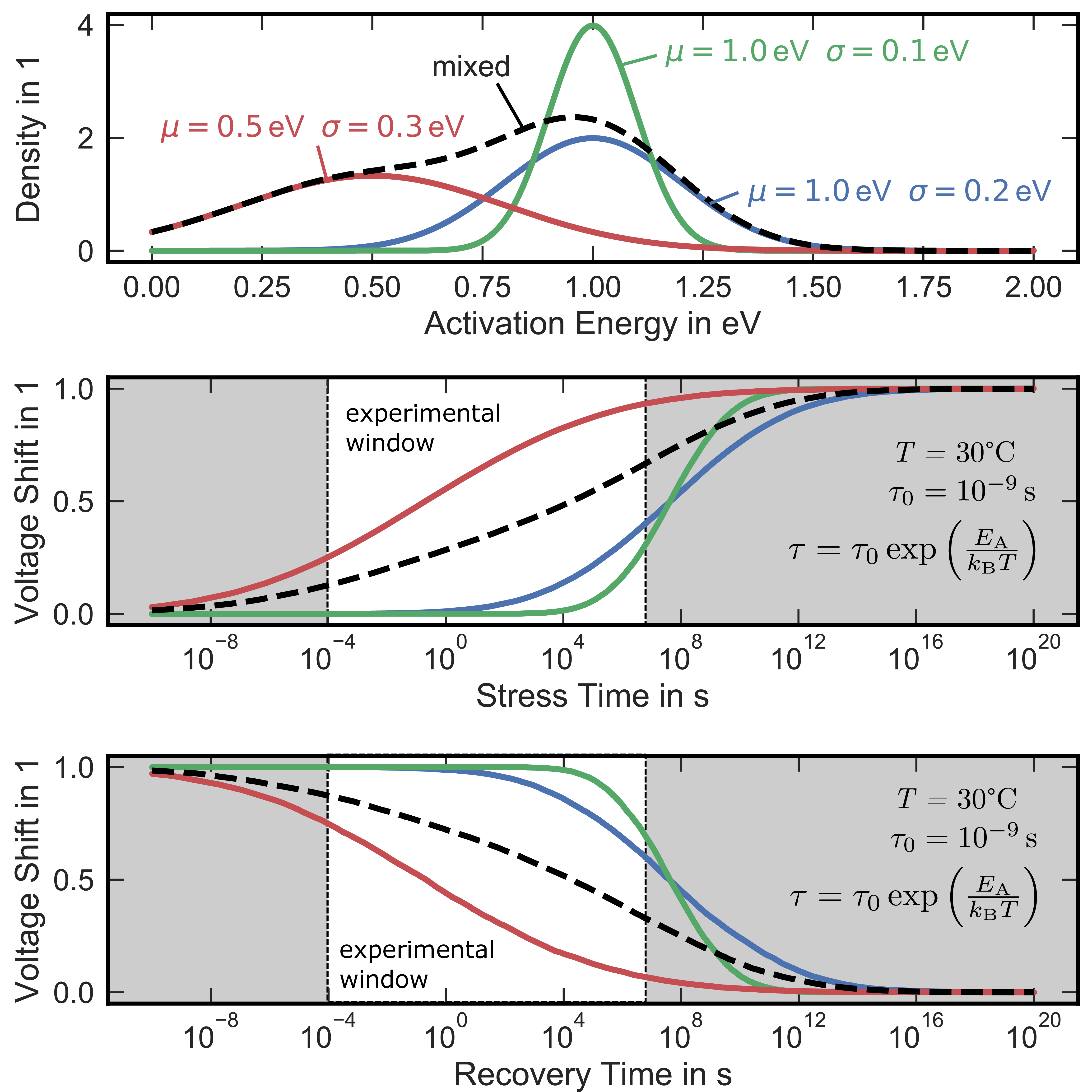
Figure 1.7: Simulated impact of distributed activation energies (top) on the observed voltage shift during stress (middle) and recovery (bottom) according to (1.4) and (1.6), respectively. The dashed black line represents a mix of the red and blue distributions, which leads to a broad dis- tribution enabling the often used power-law approximation, which is only valid within narrow experimental windows.
Instead of using (1.3), a physical way to describe the voltage shift during bias stress is given by [57]

with the stress time  , the maximum voltage shift
  as an additional fitting parameter, the parameters of the normal distribution
 and
and  , and the complimentary error function (erfc), which is given by

In addition to the capture process, the emission process during recovery can be described with a similar equation

with the recovery time  . Note that the parameters of the normal
distribution of the activation energies, and , for capture and emission processes do not necessarily correlate [46]. As can be
seen from (1.4) and (1.6), the time evolution of scales with the logarithm of the stress or recovery time, resulting in a
fundamental dependence of the measurement timing on the extracted . The strong dependence on the timing parameters of the measurement will be one of the main topics in Section 3.3.
. Note that the parameters of the normal
distribution of the activation energies, and , for capture and emission processes do not necessarily correlate [46]. As can be
seen from (1.4) and (1.6), the time evolution of scales with the logarithm of the stress or recovery time, resulting in a
fundamental dependence of the measurement timing on the extracted . The strong dependence on the timing parameters of the measurement will be one of the main topics in Section 3.3.
1.2.2 Hydrogen related defects and the hydrogen release model
Out of all the microscopic defect candidates [49, 50, 53, 54], the interaction of hydrogen with defects or precursors throughout the SiO2 is able to explain many features of the observed experimental behavior during and after an applied gate stress pulse [48, 58] for semiconductor technology based on a SiO2 dielectric. In this section, a basic overview on hydrogen related defects in amorphous SiO2 and their link to bias temperature instability is provided. Most of the information is extracted from the doctoral dissertation of Wimmer [58], where much more detailed information on hydrogen related defects is given.
Possible defect candidates
From the many possibilities of defect candidates in amorphous SiO2, which are able to explain a considerable amount of BTI features, the 3 most promising are sketched in Fig. 1.8 and described in the following:
-
• First, the oxygen vacancy (VO) as the best-studied defect in SiO2 needs to be mentioned (Fig. 1.8, left). The VO forms when an oxygen (O) atom is missing in the amorphous SiO2, which causes the two neighboring Si atoms to form a bond resulting in a strong relaxation of the surrounding network. If the oxygen vacancy traps a hole, it is converted to the E’-center defect, which has been studied intensively in numerous papers [59–63].
-
• Second, the hydrogen bridge defect (Fig. 1.8, middle), which is similar to the VO. Here, a H atom is bond to one of the silicon atoms instead of the bridging O atom. The hydrogen bridge forms when an interstitial hydrogen atom is present in the vicinity of a pre-existing VO. After overcoming a negligible barrier (
 ) [58], the
hydrogen is trapped at the position of the oxygen vacancy.
) [58], the
hydrogen is trapped at the position of the oxygen vacancy. -
• Third, the hydroxyl-E’ center as indicated in Fig. 1.8 (right). This defect forms when a H atom interacts with a two-coordinated O atom by breaking one of the Si-O bonds. It is important to note that this particular mechanism requires the presence of a strained Si-O bond, which is the case for approximately 2 % of all the Si atoms in the SiO2 as calculated by El-Sayed et al. [47]. Furthermore, the density of strained Si-O bonds is likely to increase close to the SiO2-semiconductor interface, which results in an increased likelihood of hydroxyl E’ centers in the vicinity of the SiO2-semiconductor interface.
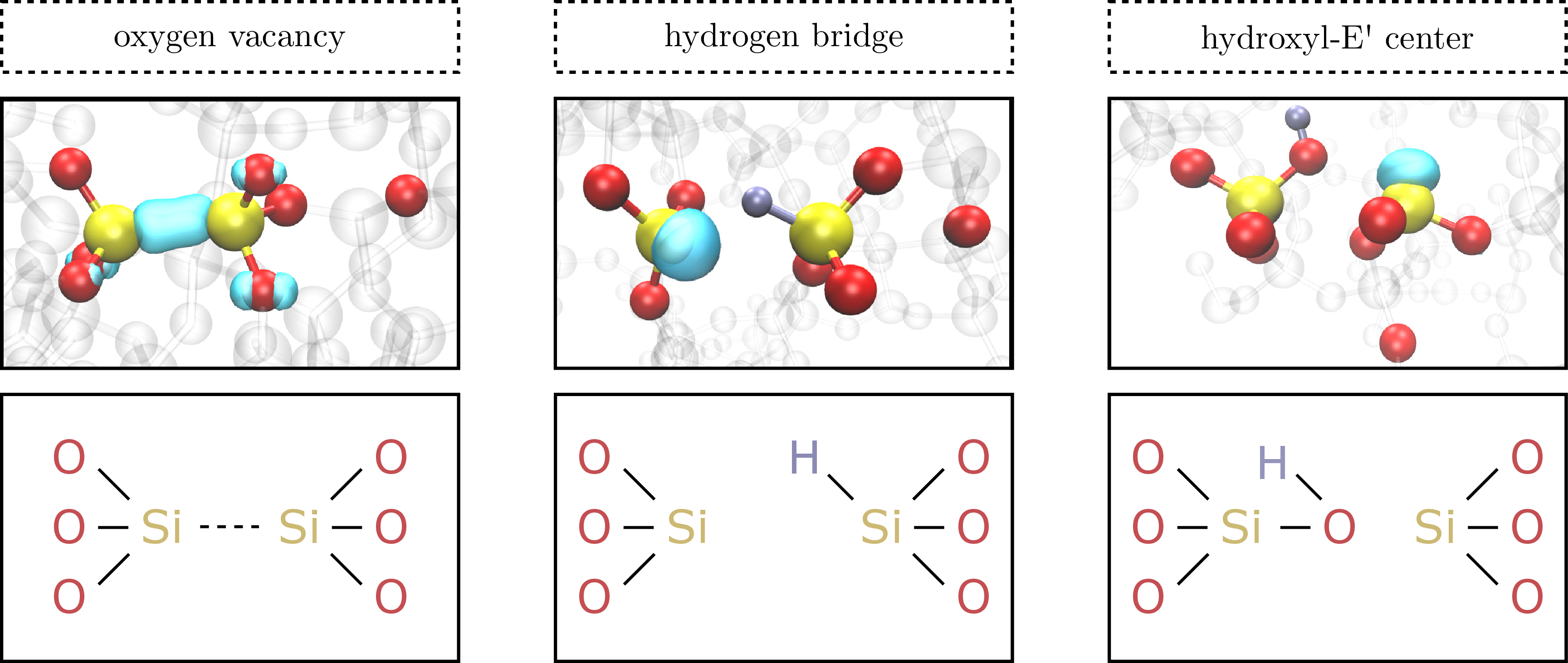
Figure 1.8: Defect candidates in amorphous SiO2. Left: the oxygen vacancy VO. The VO is able to trap a hole, which converts the VO into the well-studied E’ center. Middle: the hydrogen bridge. The defect is similar to the VO with a hydrogen atom bound to one of the Si atoms. Right: the hydroxyl E’ center. Here a hydrogen atom interacts with one of the bridging oxygen atoms by breaking one of the Si-O bonds, which requires a strained Si-O bond [58].
Hydrogen release model
Out of all atomistic models which have been proposed to explain the outcome of charge capture and emission measurements, the hydrogen release model is one of the most promising. This is mainly due to the fact, that the hydrogen release model is able to explain the recoverable as well as the permanent component, which contribute to the device degradation during BTI [64–68]. Furthermore, the hydrogen release model provides a potential explanation for the accumulation of fixed positive charges at the SiC-SiO2 interface which occurs during high-temperature processing steps, as will be discussed in Chapter 4.
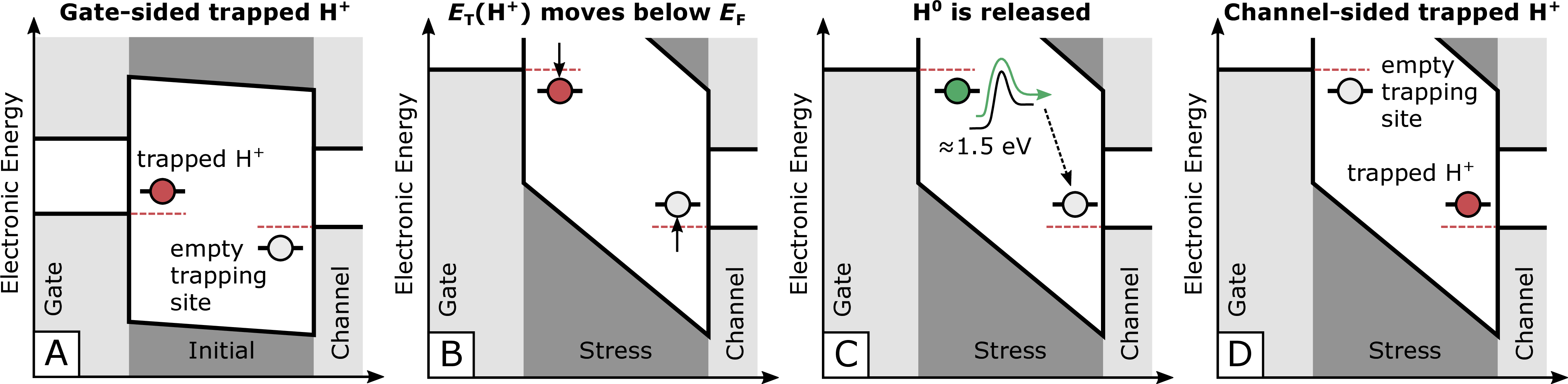
Figure 1.9: Gate-sided H-release model [69]. A trapped proton in the oxide layer close to the gate (A, left, red) may become neutralized if the energetic position of the trapped proton is shifted below the Fermi-level (B). The neutrally charged H atom can now be released by overcoming an energy barrier of approximately 1.5 eV (C). Subsequently, the neutrally charged, free H atom moves towards the SiC/SiO2 interface, where it occupies a new trapping site (D).
The hydrogen release model tries to link the permanent component, which arises during long-term gate stress, with the release of additional H from the gate into the oxide. A schematic overview of one of the possible mechanisms,
which lead to an increase of the permanent component according to the H-release model is sketched in Fig. 1.9 [69]. First, a trapped proton in the
oxide layer close to the gate electrode (A) may become neutralized if a gate potential is applied and the Fermi-level moves below the energy level of the trapped  (B). The neutrally charged hydrogen can now be released from the
trapping site by overcoming an energy barrier of approximately 1.5 eV (C). Afterwards, the released hydrogen diffuses through the oxide until it is able to occupy a new trapping site (D). It is important to note that potential
trapping sites for the H are available all over the oxide due to the amorphous nature of SiO2.
(B). The neutrally charged hydrogen can now be released from the
trapping site by overcoming an energy barrier of approximately 1.5 eV (C). Afterwards, the released hydrogen diffuses through the oxide until it is able to occupy a new trapping site (D). It is important to note that potential
trapping sites for the H are available all over the oxide due to the amorphous nature of SiO2.
1.2.3 Hydrogen hopping
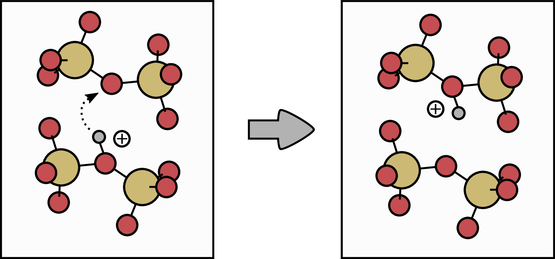
Figure 1.10: Hopping mechanism for the case of a positively charged hydrogen . Oxygen atoms are indicated in red, whereas silicon atoms are indi-
cated in yellow. The hydrogen atom (grey) moves from one bridging O (initial configuration, left) to a neighboring bridging O atom (final configuration, right). can stick to nearly all oxygen atoms, whereas the neutrally charged
hydrogen,  , can only bind to approximately 60 % of bridging O atoms
in the SiO2. The transition barrier for the hopping mechanism of the positive and neutral charge state is approximately 1.5 eV [48].
, can only bind to approximately 60 % of bridging O atoms
in the SiO2. The transition barrier for the hopping mechanism of the positive and neutral charge state is approximately 1.5 eV [48].
Although the high diffusivity of hydrogen in SiO2 allows for a very fast exchange of H to a new trapping site and should therefore not limit the rate [70], there are very low barriers for the interstitial neutral H to bind
at approximately every third O atom ( ). Therefore, neutral hydrogen
would not be able to move efficiently in the SiO2 system. However, the transport of hydrogen (either in the neutral or the positive charge state) is still possible via a so-called hydrogen
hopping mechanism, meaning the hydrogen moves from one bridging O atom to the next bridging O atom. A sketch of the hopping mechanism for the case of a positively charged hydrogen atom (proton) is given in Fig. 1.10. The positive charged H atom can stick to nearly all bridging oxygen atoms in the system, whereas the neutrally charged hydrogen can only bind to
approximately 60 % of the bridging O atoms. However, the activation energies for both transitions are similar and around 1.5 eV. Due to this, it is not clear which charge state would dominate the transport
mechanism [58].
). Therefore, neutral hydrogen
would not be able to move efficiently in the SiO2 system. However, the transport of hydrogen (either in the neutral or the positive charge state) is still possible via a so-called hydrogen
hopping mechanism, meaning the hydrogen moves from one bridging O atom to the next bridging O atom. A sketch of the hopping mechanism for the case of a positively charged hydrogen atom (proton) is given in Fig. 1.10. The positive charged H atom can stick to nearly all bridging oxygen atoms in the system, whereas the neutrally charged hydrogen can only bind to
approximately 60 % of the bridging O atoms. However, the activation energies for both transitions are similar and around 1.5 eV. Due to this, it is not clear which charge state would dominate the transport
mechanism [58].
Previous: 1 Introduction Top: 1 Introduction Next: 1.3 Methodology