« PreviousUpNext »Contents
Previous: Kurzfassung Top: Home Next: 1.2 Detrimental Effects in MOS Devices
1 Introduction
1.1 Silicon Carbide
1.1.1 Crystal Properties
Silicon carbide (SiC) is a compound semiconductor, with its atomic crystal consisting of 50 % silicon (Si) and 50 % carbon (C) atoms. Each C has exactly four Si neighbors and vice versa, with a very strong C-Si bond strength of approximately 4.6 eV, which leads to impressive material properties as will be discussed below.
Furthermore, silicon carbide is an outstanding example for polymorphism, meaning the crystal can grow in a wide range of different crystal structures (the so called polytypes), each of which exhibits unique
electrical, optical, thermal, and mechanical properties. A certain polytype is defined by the Si-C bilayer stacking sequence along the  -axis of the hexagonal close-packed system. On each Si-C bilayer (A), there are two
possible stacking sites (B, C) as illustrated in Fig. 1.1. In Ramsdell’s notation, each polytype is labeled after the number of Si-C bilayers in the unit cell and the lattice structure, which
can be cubic (C), hexagonal (H), and rhombohedral (R). The structures of the most common SiC polytypes, 3C-SiC, 2H-SiC, 4H-SiC, and 6H-SiC are shown schematically in Fig. 1.2. The respective lattice properties are given in Table 1.1. In Fig. 1.2, Si atoms are indicated in green, whereas C atoms are shown in black.
-axis of the hexagonal close-packed system. On each Si-C bilayer (A), there are two
possible stacking sites (B, C) as illustrated in Fig. 1.1. In Ramsdell’s notation, each polytype is labeled after the number of Si-C bilayers in the unit cell and the lattice structure, which
can be cubic (C), hexagonal (H), and rhombohedral (R). The structures of the most common SiC polytypes, 3C-SiC, 2H-SiC, 4H-SiC, and 6H-SiC are shown schematically in Fig. 1.2. The respective lattice properties are given in Table 1.1. In Fig. 1.2, Si atoms are indicated in green, whereas C atoms are shown in black.
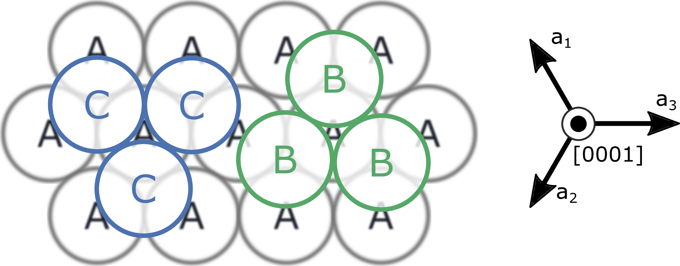
Figure 1.1: Possible stacking sites of the SiC crystal along the -axis. Each site (A, B, and C) represents a bilayer of Si-C atoms along the -axis of the hexagonal close-packed system. The most common polytypes, 3C-SiC (ABCA),
2H-SiC (ABA), 4H-SiC (ABCBA), and 6H-SiC (ABCACBA) are shown schematically in Fig. 1.2.
Unlike the silicon crystal, the silicon carbide crystal has lattice sites which differ in their structures of nearest neighbors. These lattice sites can either be hexagonal sites or cubic sites. In Fig. 1.2, those sites are indicated with "h" for a hexagonal or "c" for a cubic lattice site. Cubic and hexagonal sites mainly differ in their position of second-nearest neighbors, which results in different electric fields at the specific site. Therefore, energy levels of impurities, dopants, or point defects depend on the occupied lattice site of the defect/dopant (the so-called site-effect [1]). The relative concentration of hexagonal or cubic sites furthermore depends on the polytype: while only cubic sites are present in 3C-SiC, 4H-SiC has one hexagonal and one cubic site, whereas 6H-SiC has one cubic and two hexagonal sites.
Out of the hundreds of available polytypes, 4H-SiC has been almost exclusively employed for power devices. This is mainly due to the following two reasons:
-
• First, as a result of the high electron mobility
 and critical breakdown field
  , the Baliga figure of merit (BFOM)
 which defines the material parameters which can be used to minimize the conduction losses in power FET’s [2, 3], is significantly higher for 4H-SiC than for most other polytypes, as also indicated in Table 1.1.
-
• Second, the availability of high-quality, single-crystalline 4H-SiC wafers with large diameters of up to 6 inch (by 2017), allows for higher yields and cost-reduction of commercial devices. Even though other polytypes, like 2H-SiC, might have an even higher mobility than 4H-SiC (as suggested by theoretical calculations [4]), no feasible substrates are available due to the highly complex growth process and polytype control of SiC crystals.

Since all investigated devices in this thesis are based on 4H-SiC, the abbreviation "SiC" refers to the 4H polytype of SiC in all subsequent sections of this work unless otherwise stated.
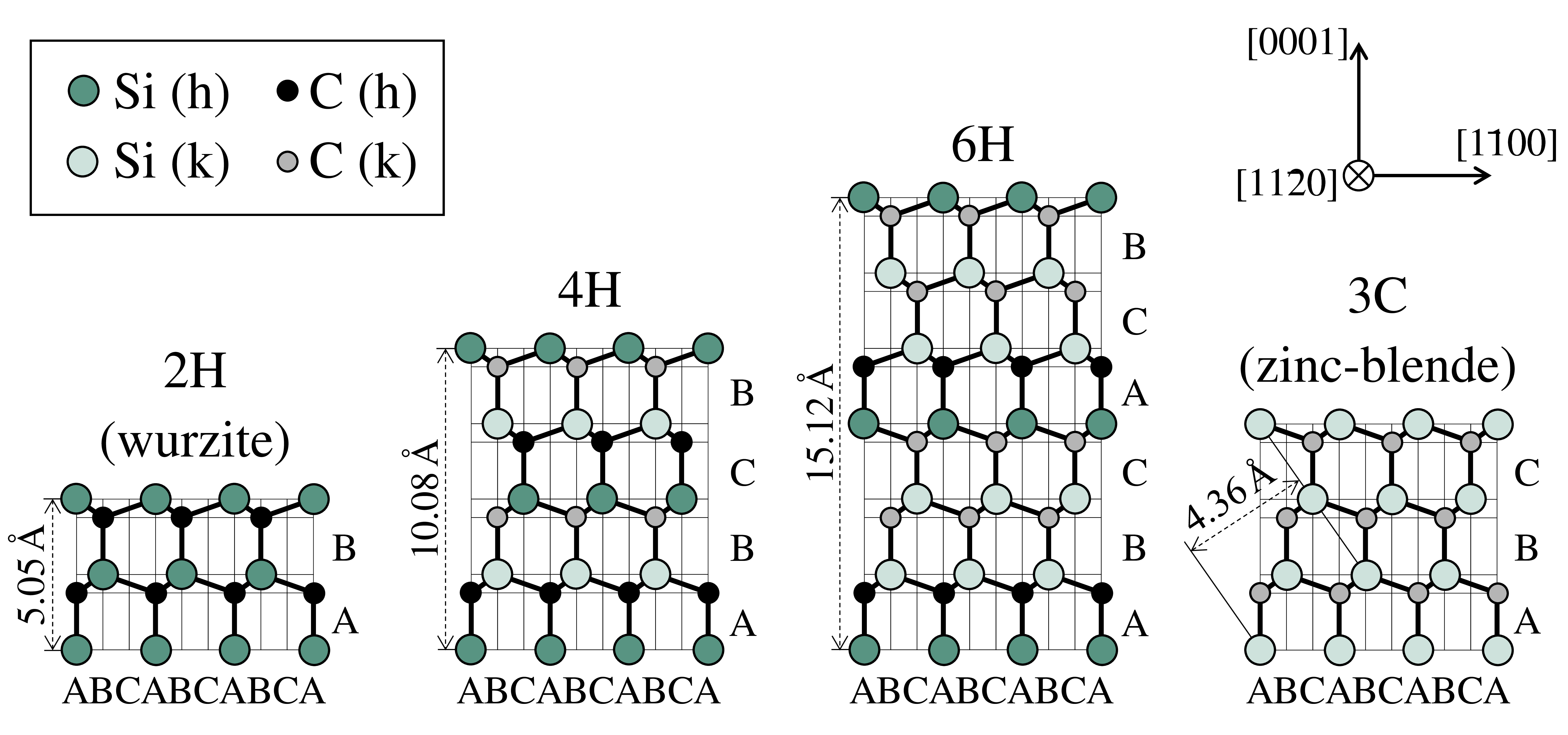
Table 1.1: Properties of the most simple SiC polytypes at 300 K [4, 6, 7].
| Property | 2H-SiC | 3C-SiC | 4H-SiC | 6H-SiC |
| Stacking sequence | AB | ABC | ABCB | ABCACB |
Lattice constant  |
5.05 | n.a. | 10.05 | 15.12 |
Lattice constant  |
3.07 | 4.36 | 3.07 | 3.07 |
| Band gap energy (eV) | 3.33 | 2.39 | 3.26 | 3.02 |
Electron mobility  ( ( ) ) |
4H a a |
1000 | 1020 | 450 |
Electron mobility  () () |
4H a a |
1000 | 1200 | 100 |
| Hole mobility () |
- | 100 | 120 | 100 |
| BFOM (relative to Si) | n.a. | 61 | 626 | 63 |
1.1.2 Peculiarities of silicon carbide wafers
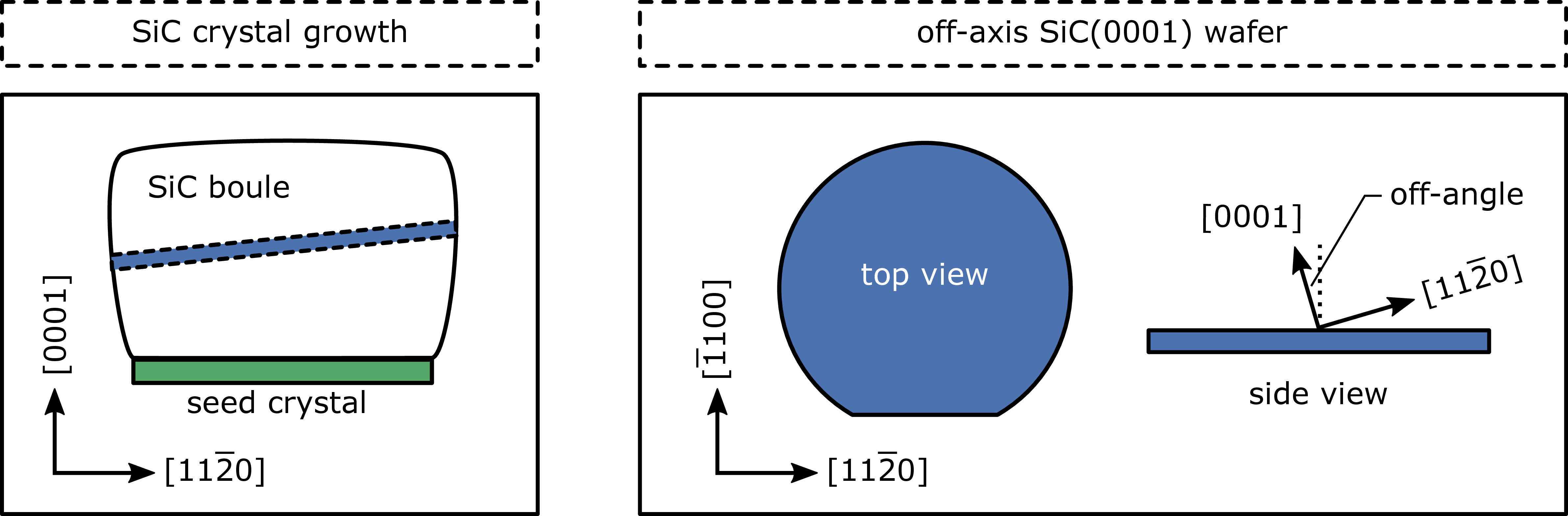
Silicon carbide bulk crystals (SiC boules) are usually grown along the ![\( [0001] \)](lateximages/7D51FA43FD4DCF53EDD840D4431AA20C.svg) direction from a seed crystal using the
sublimation growth technique, which was first introduced by Lely in 1955 [8] and later optimized by Tairov and Tsvetkov (modified Lely method) [9, 10]. The growth rate of SiC boules using seeded sublimation growth is
around 1 mm/h. The final length of the SiC boule is usually between 30 mm and 50 mm. Compared to silicon ingots, the complicated growth technique in combination with the slow growth rate and the
significantly shorter length of the boules, which is in the range of several meters for silicon and some centimeters for SiC, are the main reasons for the tremendous costs of approximately
direction from a seed crystal using the
sublimation growth technique, which was first introduced by Lely in 1955 [8] and later optimized by Tairov and Tsvetkov (modified Lely method) [9, 10]. The growth rate of SiC boules using seeded sublimation growth is
around 1 mm/h. The final length of the SiC boule is usually between 30 mm and 50 mm. Compared to silicon ingots, the complicated growth technique in combination with the slow growth rate and the
significantly shorter length of the boules, which is in the range of several meters for silicon and some centimeters for SiC, are the main reasons for the tremendous costs of approximately  for one 150 mm high-quality SiC
substrate (by 2018).
for one 150 mm high-quality SiC
substrate (by 2018).
In general, the process for the production of silicon carbide wafers from the boule crystals is similar to that used for silicon wafers. The main peculiarity of SiC wafers arises from the fact that silicon carbide wafers are sliced
off-axis (off-angle) from the cylindrical boules. The whole process is sketched in Fig. 1.3 (left). Fig. 1.3
(right) shows the resulting off-axis 4H-SiC(0001)-wafer, which is usually tilted 4° toward the ![\( [11\bar {2}0] \)](lateximages/F4D0F6542B1D4AECD93D3CAC82ACC347.svg) (or ) direction.
(or ) direction.
The main reason for the off-axis cut of the SiC wafers is to enable polytype preservation during the high-quality homoepitaxial growth process [6, 11] as indicated in Fig. 1.4. Without an off-axis wafer cut, all stacking information of the polytype is lost and two arrangements, A or B, are possible for the atomic bilayer, which follows C. Due to
the step edges, which arise on the surface of an off-axis wafer, only a single possible bond configuration remains (B) [5, 6] because the stacking information is transfered along the crystal growth direction. Fig. 1.5 provides a schematic illustration of the growth modes on an off-axis 4H-SiC wafer during the epitaxial process. The microscopic crystal growth takes place along the step edges,
which results in a macroscopic growth along the -axis. Although the off-axis wafer is of fundamental importance for the polytype
control, the off-orientation results in an increased surface roughness at the SiC-silicon dioxide (SiO2) interface (the so-called step-bunching), since all step edges are transfered to the surface of the wafer. In the
final device, an increased interface roughness along the surface on which the inversion channel forms, might result in a decreased mobility. Therefore several manufacturers try to avoid the step-bunching on the plane by using trench devices, which also save
expensive wafer area, as will be discussed in Section 1.3.2.
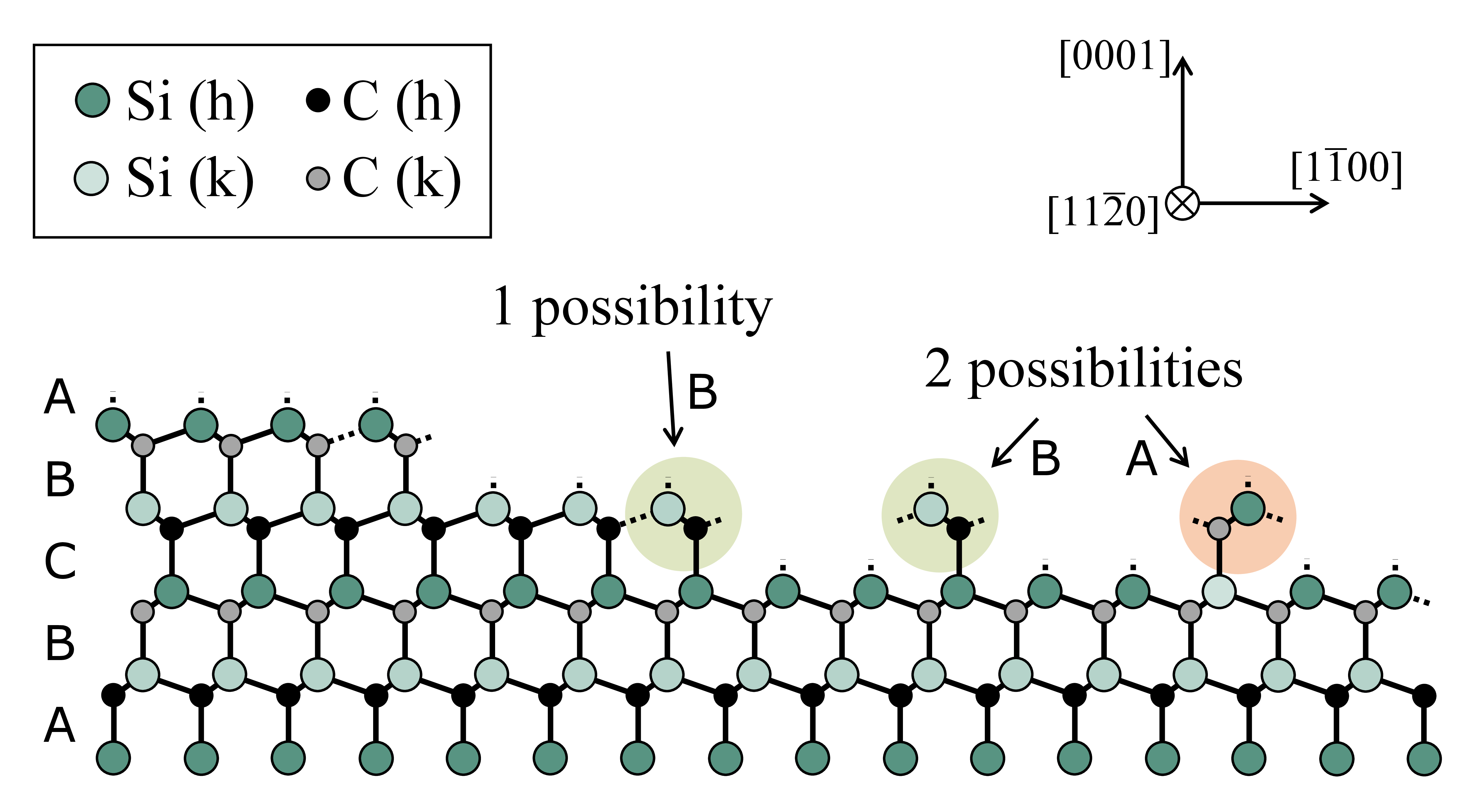
Figure 1.4: The basic principle of polytype control. Without an off-axis wafer cut, two arrangements (A or B) for the next atomic bilayer are possible after bilayer C since every information about the stacking sequence is lost. Due to the step edges, only a single possible bond configuration remains (B) [5, 6] and the stacking information is available in the crystal growth direction.

Figure 1.5: Schematic illustration of the growth modes on an off-axis 4H-SiC wafer. The off-axis cut allows for a preservation of the polytype as indicated in Fig. 1.4 [5, 6].
1.1.3 Benefits for power devices
As a wide band gap (WBG) semiconductor, 4H-SiC promises superior performance for power device operation due to the 10 times higher breakdown field and 3 times higher thermal conductivity than silicon [12–15]. The higher
breakdown field allows for a ten times reduction in the drift layer thickness, which enables a decrease of the on-resistance  by more than two orders of magnitude.
Furthermore, minority carrier charge storage is reduced, allowing for operation at elevated switching frequencies and reduced switching losses. Together with the high thermal conductivity, which enhances heat dissipation and
furthermore allows device operation at high temperatures above 400 °C [16–18], SiC is the most promising candidate for high-power electronic semiconductor devices [19].
by more than two orders of magnitude.
Furthermore, minority carrier charge storage is reduced, allowing for operation at elevated switching frequencies and reduced switching losses. Together with the high thermal conductivity, which enhances heat dissipation and
furthermore allows device operation at high temperatures above 400 °C [16–18], SiC is the most promising candidate for high-power electronic semiconductor devices [19].
Another important aspect of SiC is its native oxide SiO2, which is identical to silicon based devices. Therefore, a high amount of device processing knowledge can be transfered to the processing of SiC based devices. However, several significant differences like the handling of transparent wafers, necessary high temperature furnaces, low diffusion constants, and novel annealing techniques remain, which is why producing high-quality and reliable SiC devices remains challenging. A comparison of important material parameters for 4H-SiC and other semiconductor materials is provided in Tab. 1.2.
Table 1.2: Material properties of 4H-SiC compared to other semiconductors [2, 6, 20–23].
| Property | 4H-SiC | Si | GaAs | Diamond | GaN |
| Band gap energy (eV) | 3.26 | 1.12 | 1.43 | 5.45 | 3.45 |
Breakdown field  |
3.2 | 0.3 | 0.4 | 5.7 | 3.0 |
Therm. conductivity  |
4.9 | 1.5 | 0.46 | 22 | 1.3 |
 drift velocity drift velocity  |
2.2 | 1.0 | 1.0 | 2.7 | 2.2 |
mobility  |
1200 | 1500 | 8500 | 2200 | 1250 |
Melting point  |
2830 | 1420 | 1240 | 4000 | 2500 |
| BFOM (relative to Si) | 626 | 1 | 16 | 27000 | 650 |
Previous: Kurzfassung Top: Home Next: 1.2 Detrimental Effects in MOS Devices