« PreviousUpNext »Contents
Previous: 1.3 Methodology Top: Home Next: 2.2 Investigated devices
2 On the first Component: the Subthreshold Hysteresis
2.1 Occurrence of the hysteresis
State of the art power MOSFETs based on SiC show a drain current sweep hysteresis between gate voltage  sweeps from accumulation to inversion and vice
versa. An example of this phenomenon is given in Fig. 2.1 for a sweep from −5 V to 5 V
(up-sweep, blue) and from 5 V to −5 V (down-sweep, red) at a fixed drain voltage
sweeps from accumulation to inversion and vice
versa. An example of this phenomenon is given in Fig. 2.1 for a sweep from −5 V to 5 V
(up-sweep, blue) and from 5 V to −5 V (down-sweep, red) at a fixed drain voltage  of 0.1 V. The hysteresis is mainly
visible in the subthreshold regime where the on-resistance
of 0.1 V. The hysteresis is mainly
visible in the subthreshold regime where the on-resistance  of the device is still in the range of several
megaohms and becomes less significant as the gate voltage approaches the threshold voltage
of the device is still in the range of several
megaohms and becomes less significant as the gate voltage approaches the threshold voltage  . Above , which is approximately at
  for the tested device, the
hysteresis disappears completely (inset).
for the tested device, the
hysteresis disappears completely (inset).
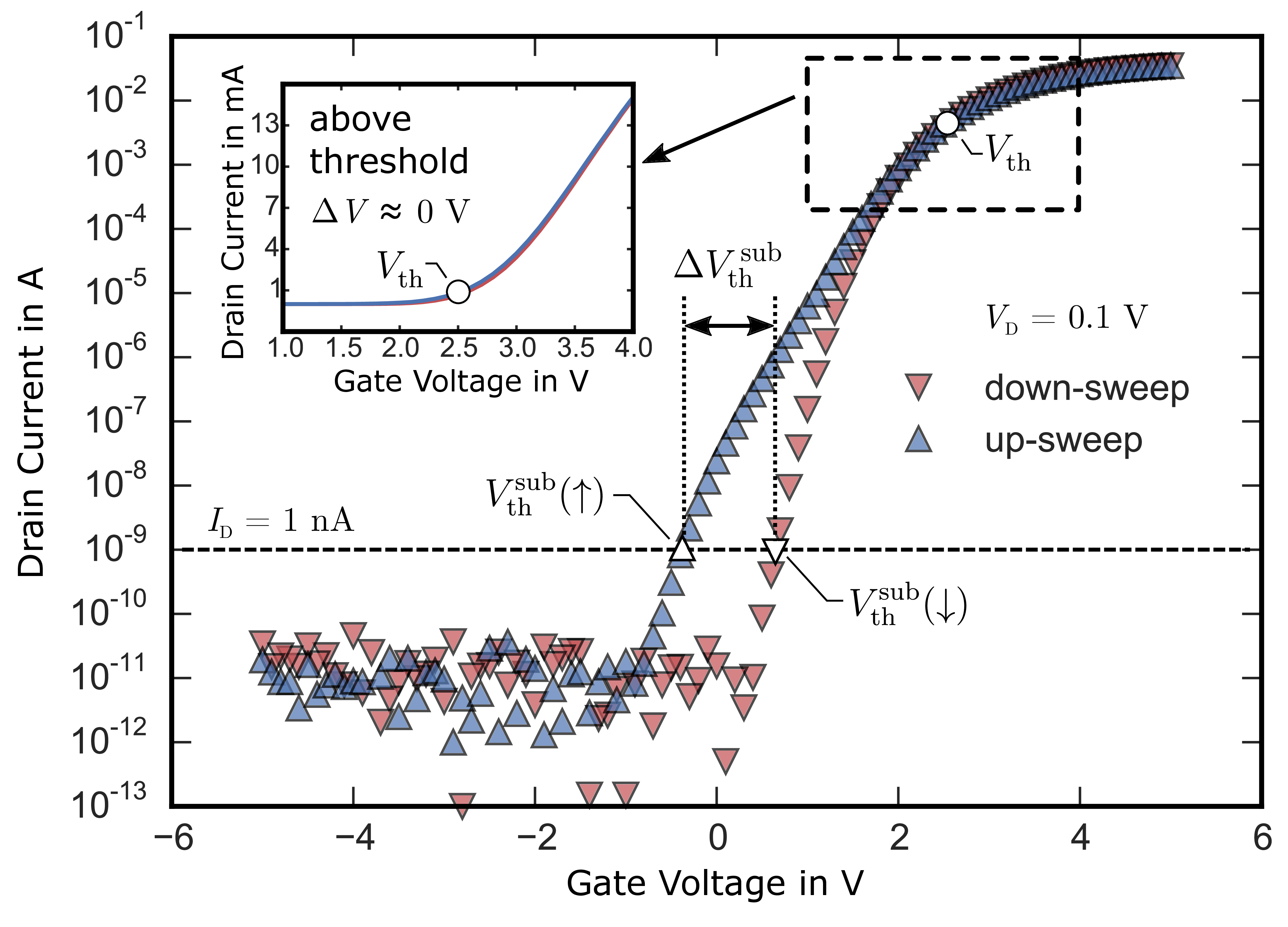
Figure 2.1: Sweep hysteresis between the up-sweep starting at −5 V (blue, rectangles up) and the down-sweep starting at 5 V (red, rectangles down). The dashed horizontal line represents the readout current
of  at 1 nA. The inset shows the input char-
acteristics in linear scale above the threshold voltage where the hysteresis effect vanishes.
at 1 nA. The inset shows the input char-
acteristics in linear scale above the threshold voltage where the hysteresis effect vanishes.
In the next sections, we define the gate voltage at which the drain current  reaches 1 nA, at a fixed drain voltage
of 0.1 V, as subthreshold voltage
reaches 1 nA, at a fixed drain voltage
of 0.1 V, as subthreshold voltage

Note that the difference between and is the extraction current at the drain terminal.
is extracted at a drain current of
1 µA and represents the "real" threshold voltage of the devices. On the other hand, is extracted in the subthreshold regime at a
drain current of 1 nA. The subthreshold voltage depends on the sweep direction as indicated in Fig. 2.1. A gate sweep in the positive
direction from accumulation to inversion (up-sweep,  ) starting at
  results in a
  of −400 mV, whereas
a gate sweep in the negative direction from inversion to accumulation (down-sweep,
of −400 mV, whereas
a gate sweep in the negative direction from inversion to accumulation (down-sweep,  ) starting at
  leads to a
  of
of  . The total hysteresis between the
up-sweep () and the down-sweep () is expressed as a subthreshold voltage
shift
. The total hysteresis between the
up-sweep () and the down-sweep () is expressed as a subthreshold voltage
shift 

In the example given in Fig. 2.1, this corresponds to  .
.
Although the presence of is an outstanding difference between
state-of-the-art SiC and Si based MOSFETs, the effect is poorly investigated and little to no literature on this specific topic is available. However, for a comprehensive knowledge on performance and reliability limiting factors of
state-of-the-art and future devices, a deeper understanding on the subthreshold hysteresis mechanism is required.
Previous: 1.3 Methodology Top: Home Next: 2.2 Investigated devices