« PreviousUpNext »Contents
Previous: 2.6 Charge pumping Top: 2 On the first Component: the Subthreshold Hysteresis Next: 2.8 Hysteresis on devices by various manufacturers
2.7 Possible atomic origin
Ion contamination as an origin of the  is excluded by three reasons. First, the capture
and emission times are too fast for ion movement. Second, the hysteresis is already observed and nearly unchanged at low temperatures where ion movement is suppressed (e.g. −60 °C). Third, the sign of caused by typical ion contamination such as
K+ or Na+ would be inverted (e.g. a negative
is excluded by three reasons. First, the capture
and emission times are too fast for ion movement. Second, the hysteresis is already observed and nearly unchanged at low temperatures where ion movement is suppressed (e.g. −60 °C). Third, the sign of caused by typical ion contamination such as
K+ or Na+ would be inverted (e.g. a negative  for positive bias stress) [118].
Electrically detected magnetic resonance (EDMR) measurements by Gruber et al. in combination with density functional theory (DFT) simulations by Cottom et al. demonstrate that the dominant hyperfine EDMR spectrum at the SiC-SiO2 interface of Si-face MOSFETs (see. Fig. 2.32) can be understood in terms of carbon dangling bonds (PbC centers) [5, 119, 120]. The atomic configuration of this defect is shown schematically in Fig. 2.33. Recent work by Gruber shows an increased PbC signal on a-face devices indicating an increased density of these traps [121]. Due to this, a possible origin of the observed difference in hysteresis could involve the increased carbon density at the surface of the a-face and therefore a higher density of PbC centers at the SiC-SiO2 interface. These results fit well to the difference in trap density extracted via the sweep hysteresis and charge pumping measurements. Therefore, PbC centers are suggested as the most promising defect candidates for the subthreshold hysteresis effect, although this is still based on limited literature and further studies on the electrical responses of carbon dangling bonds are needed.
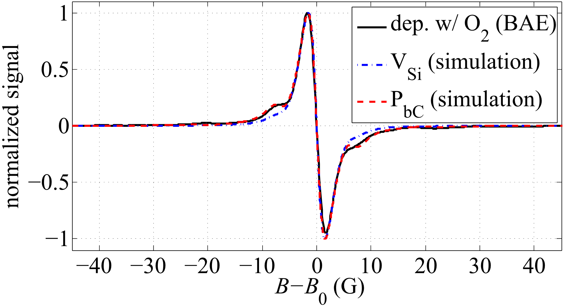

Figure 2.33: Schematic view of the silicon vacancy (VSi) and the PbC that were considered for comparison with the EDMR measurements [5, 119]. 1) VSi on a terrace, 2) PbC at a terrace, 3) PbC on a step edge, 4) VSi in the layer beneath the interface. Left: view along the [1120]-direction. Right: view along the [0001]-direction [5].
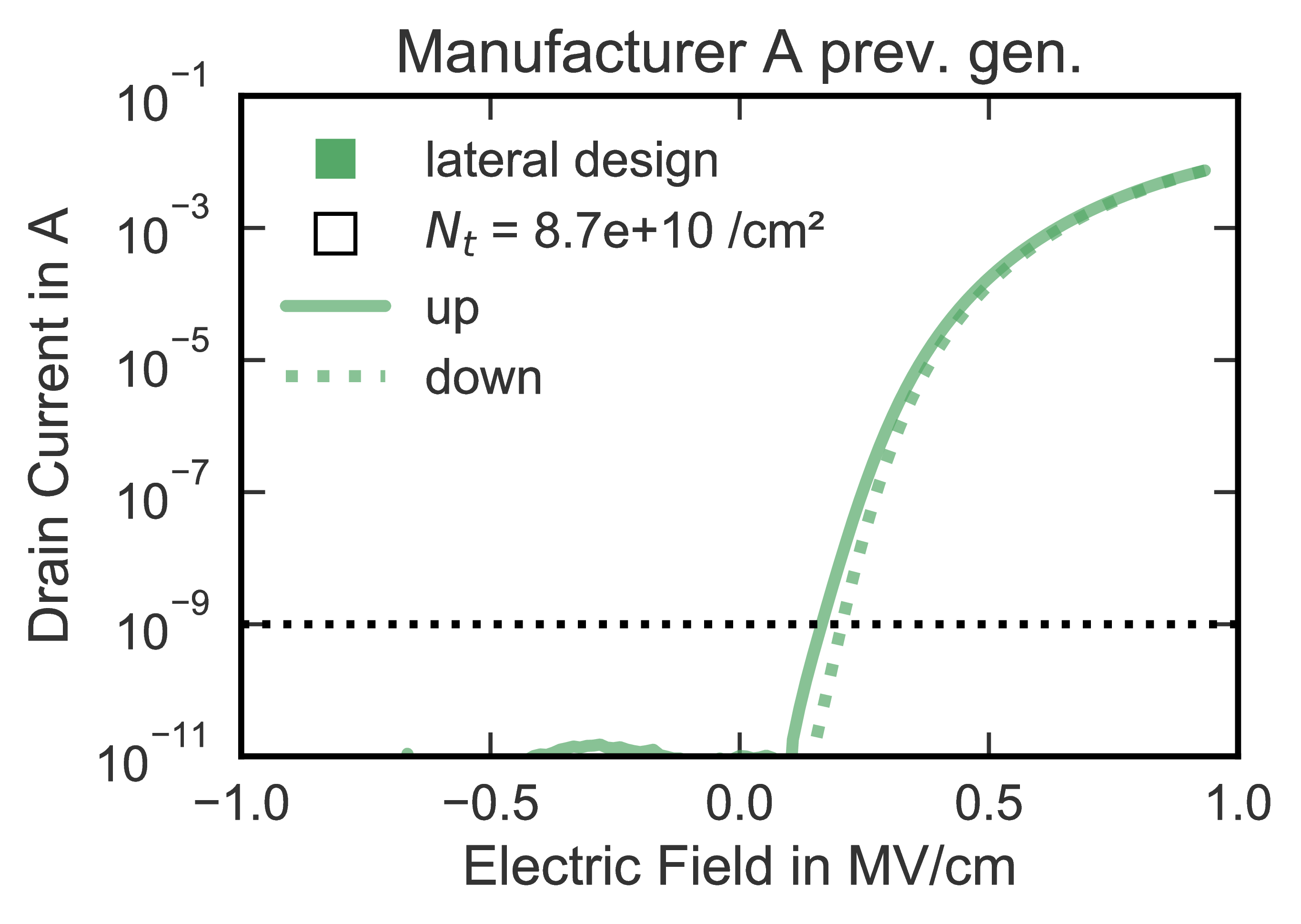
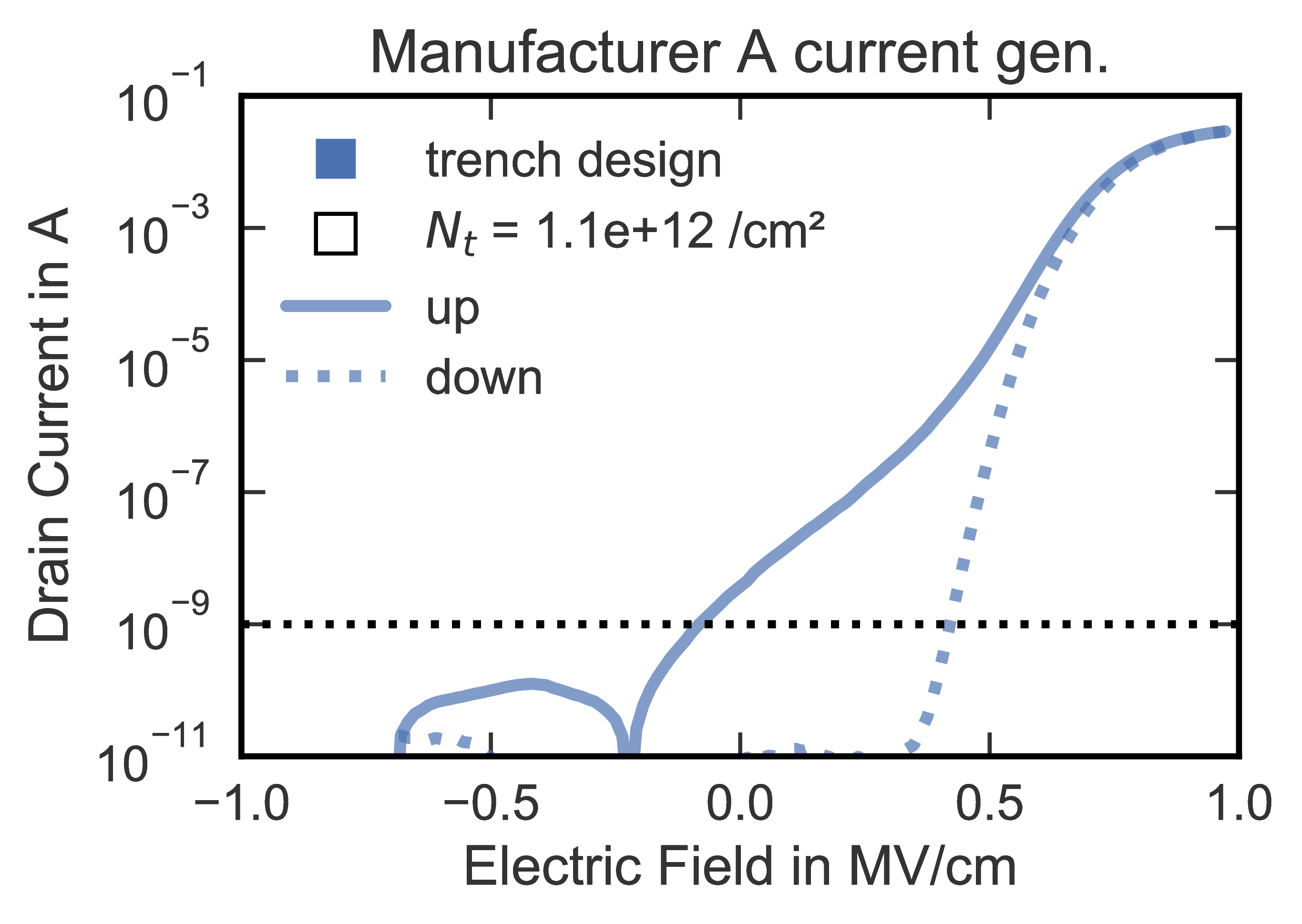
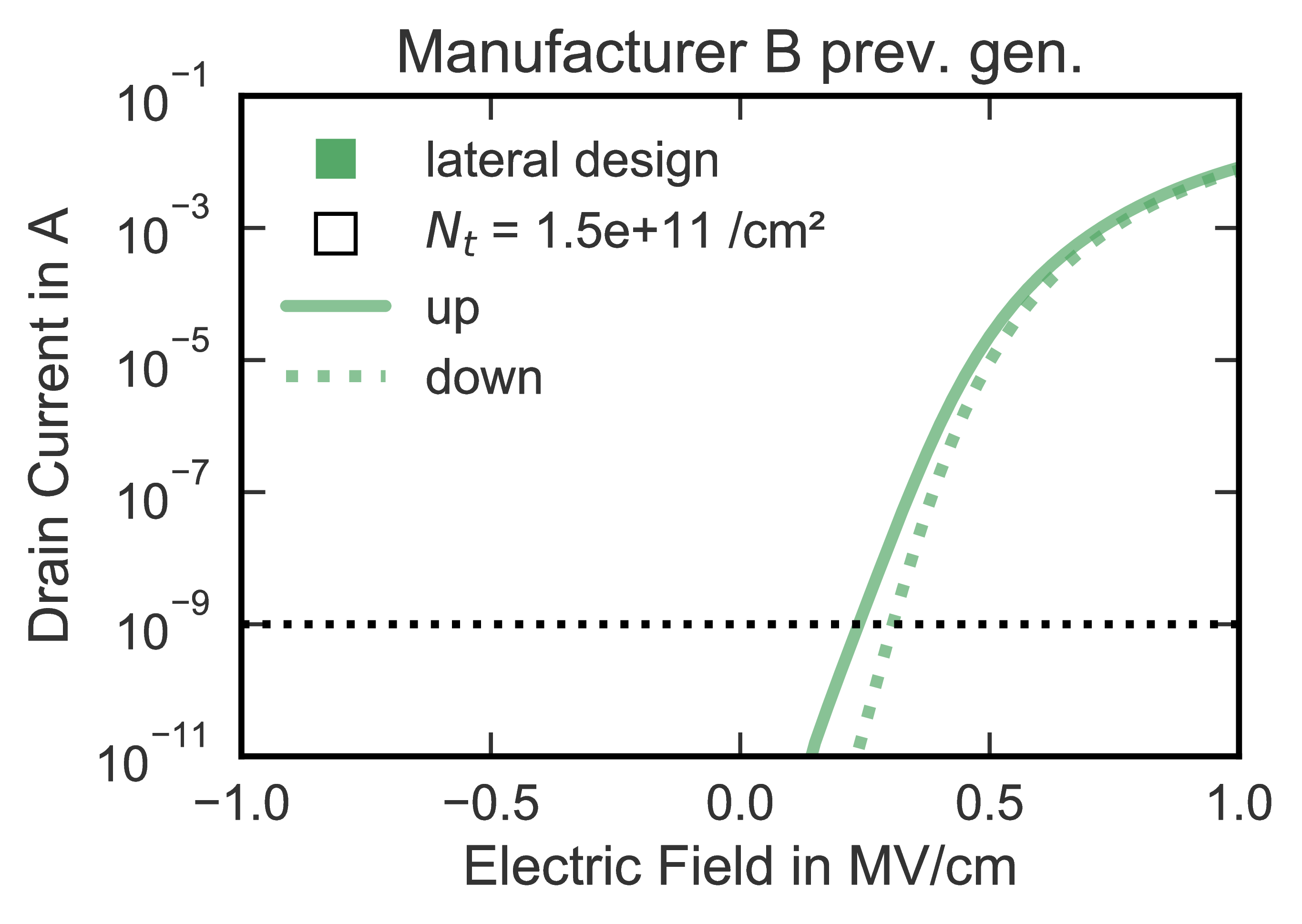
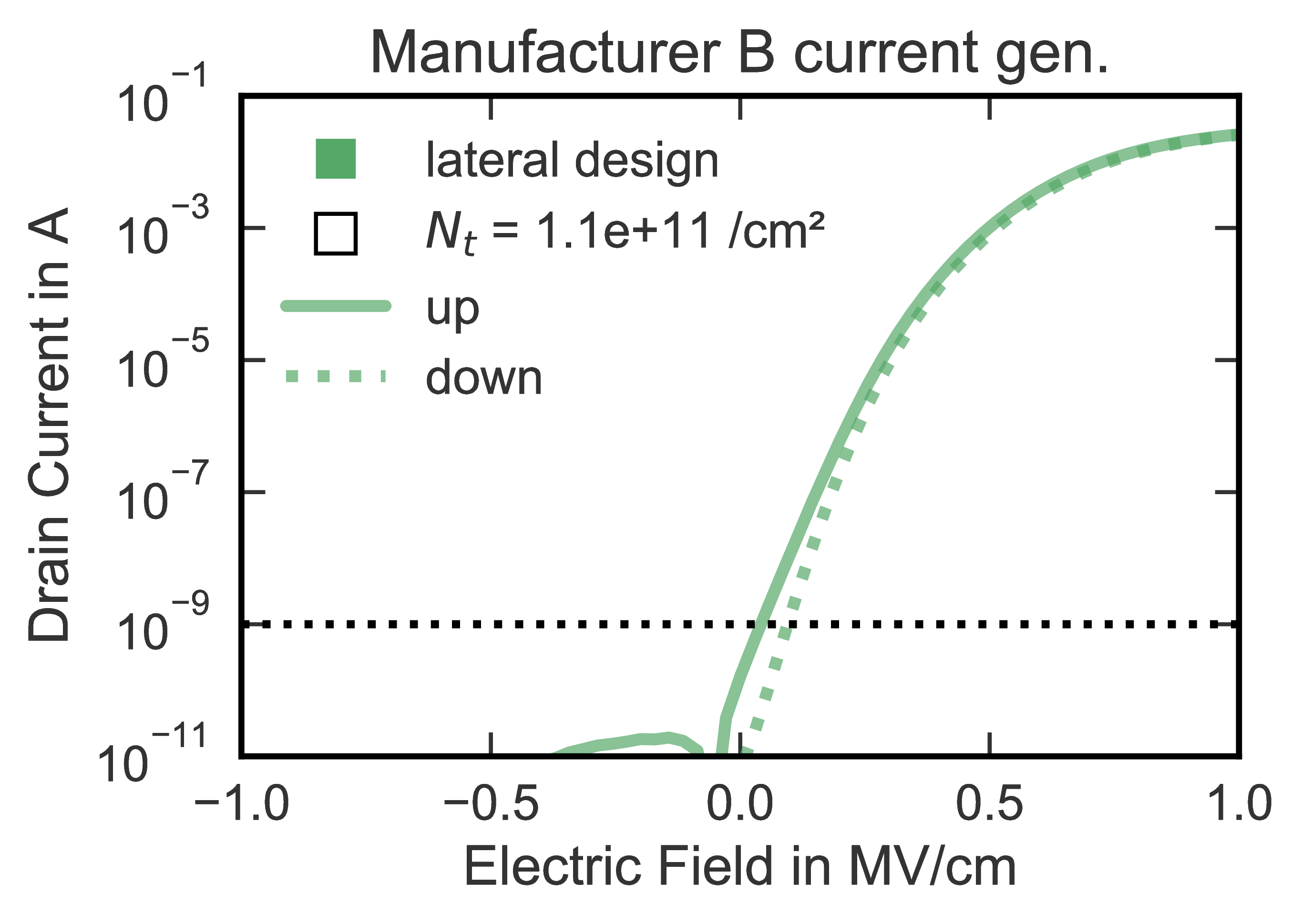
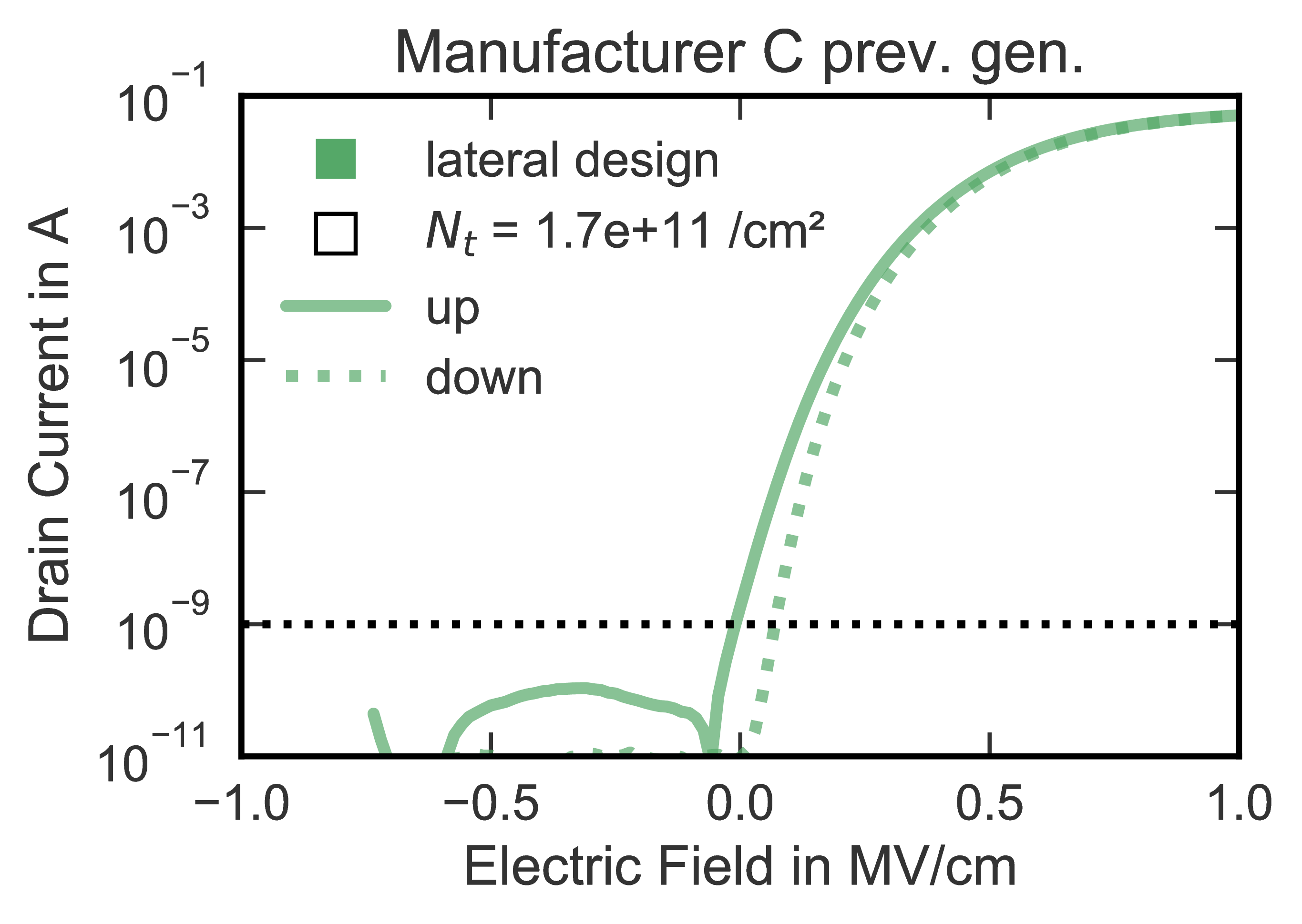

Figure 2.34: Transfer characteristics from devices of three different manufacturers. The previous device generation is given on the left, whereas the current device generation is given on the right side. Devices with the inversion
channel on the ![\( [0001] \)](lateximages/7D51FA43FD4DCF53EDD840D4431AA20C.svg) -plane are indicated in green, whereas devices with
the inversion channel along the
-plane are indicated in green, whereas devices with
the inversion channel along the  -axis (trench design) are indicated in blue. Trench devices show an increased hysteresis
and therefore an increased number of trapped charges by approximately one order of magnitude.
-axis (trench design) are indicated in blue. Trench devices show an increased hysteresis
and therefore an increased number of trapped charges by approximately one order of magnitude.
Previous: 2.6 Charge pumping Top: 2 On the first Component: the Subthreshold Hysteresis Next: 2.8 Hysteresis on devices by various manufacturers