Next: 1.2.2 Classification and Designs Up: 1.2 Three-Dimensional Integration Previous: 1.2 Three-Dimensional Integration
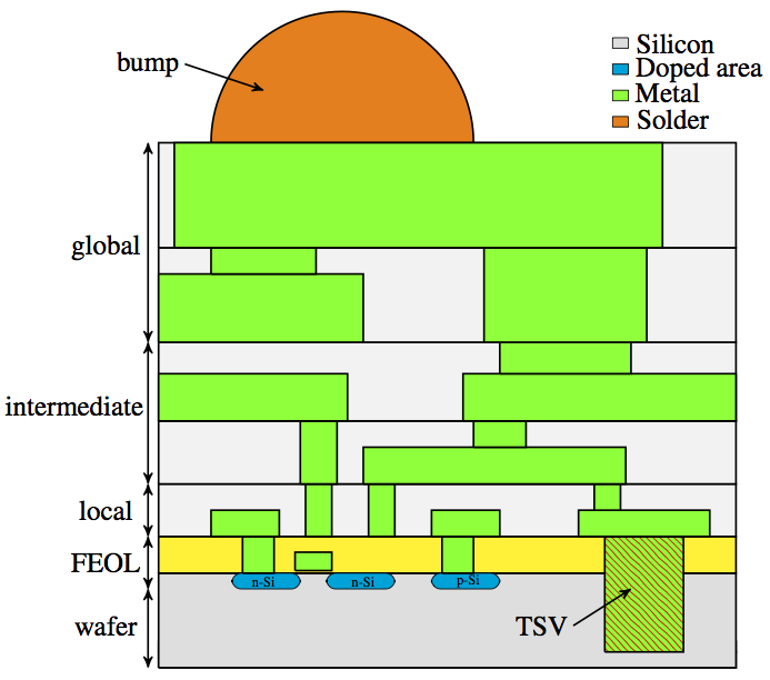
In 3D integration, the communication among the stacked sections of the chip requires vertical interconnections [131]. The interconnect design in 3D integration is organized in a hierarchical manner, which is related to the industrial semiconductor supply chain, as depicted in 1.5. The wafer fabrication stage requires 3D connections from narrow and short local interconnects between electrical components of the circuit block to wide and long intermediate and global interconnect layers in order to connect different circuit blocks [84]. Connections between adjacent interconnect planes are realized through "vias" which allow for the 3D stacking of interconnect levels. The most popular and innovative type of 3D technology at this stage is a special type of "via", which penetrates through an entire silicon wafer, known as a through silicon via (TSV). At the wafer-level packaging and assembly stages, different bond-pad and package interconnect structures are used, such as wire bonding, solder bumps, metal pillars, and redistribution layers (RDLs).