Next: 1.3.3 Reliability Issues Up: 1.3 Interconnect Technologies Previous: 1.3.1 Through Silicon Vias Approaches
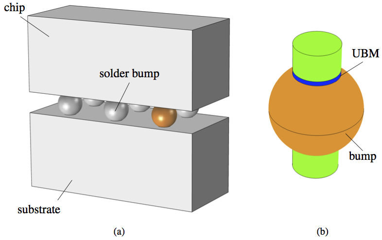
Wire bonding is considered the most common technique for making interconnections between an IC and its packaging during the fabrication process. Due to the increased number of dies on a SiP, bonding wires can exhibit parasitic impedance and reduced interconnect bandwidth [122]. The introduction of new interconnect technologies permits to overcome the limitations of wire bonding. The typical communication mechanism among different dies or packages of the 3D stack is realized in a flip-chip manner through solder bumps, which is in contrast to the older wire bonding technology. In particular, a greater number of dies can be integrated by employing an area array of solder bumps to connect silicon chips to the first level packaging substrates [34].
Flip-chip is a 3D-WLP bonding technique which provides the connections among the levels of the 3D stack with solder bumps [153]. Once the ICs are created on the wafer, the chip pads are metallized on the top side of the ICs during the final wafer processing step [122]. Solder bumps are deposited on each of the chip pads. Then, in order to attach the wafer to another substrate, it is "flipped" or faced down and aligned so that the solder bumps are facing the bond pads on the substrate [122], as depicted in 1.9. Bumps are remelted and, in most cases, the mounted chip is underfilled with an electrically non-conductive material.
1.9 shows the details of a solder bump structure. The bump is typically realized as a solder interconnect, formulated in binary, ternary or quaternary alloy system with different combinations of tin (Sn), silver (Ag), and Cu [31]. A thin film under-bump-metallization (UBM), which is usually made of nickel (Ni), is introduced on the chip bond pads during the solder bumping process in order to separate the bump from the surrounding metal interconnect lines on the chip side. The selection of an appropriate UBM layer becomes a key process for the development of reliable flip-chip solder bumps. The main function of the UBM layer is to reduce the current crowding effect and maximum hot-spot temperature near the contact between the bump and the surrounding metal line in order to improve the lifetime of the technology [32]. In turn, on the substrate side, the metallic bond pad enables the contact between the solder bump and the metallization on the substrate.
Solder bumps constitute important elements of the 3D stacking process since they serve several functions in the flip-chip assembly [126]. Bumps provide both the electrically and thermally conductive paths to carry electrical current and heat from the chip to the substrate. In addition, they guarantee the mechanical support during the mounting of the die to the substrate, because they mitigate the mechanical strain between chip and substrate. Furthermore, the height of the solder bump core provides the necessary space between successive layers, preventing the electrical contact between their conductors.
The typical diameter of a flip-chip solder bump for 3D-WLP technologies is in the range from 100μm to 200μm [122]. Advancements in the bonding processing technique have resulted in a decreased diameter of solder bumps to a range between 30μm and 50μm. In recent years, bumps containing a plastic solder ball have been introduced in order to extend the reliability of the flip-chip technology used in electronic products [158]. However, the trend of miniaturization continues to scale down the bump diameter, increasing current density in the solder bump.
 |