Next: 5. Case Study of Electromigration in Interconnects Up: 4.3 Simulation Implementation in COMSOL Multiphysics Previous: 4.3.1 Finite Element Method Procedure in COMSOL Multiphysics
Electromigration is a complex physical phenomenon governed by various PDEs and involves an electro-thermo-mechanical analysis. The models presented in Chapter 3 describe the electromigation phenomenon well and show its peculiarity to be a multiphysics problem. The solutions of these models cannot be easily obtained by employing analytical approaches because of the different physical effects related to electromigration. Furthermore, the impact of complex interconnect structures and constraints imposed by the surrounding layers on the derivation of analytical solutions does not produce proper results. For this purpose, FEM can be adopted to obtain numerical solutions of the problem. In particular, a FEM-based software, such as COMSOL Multiphysics® [38], is able to solve the coupled-field analysis and handle complicated 2D and 3D geometries.
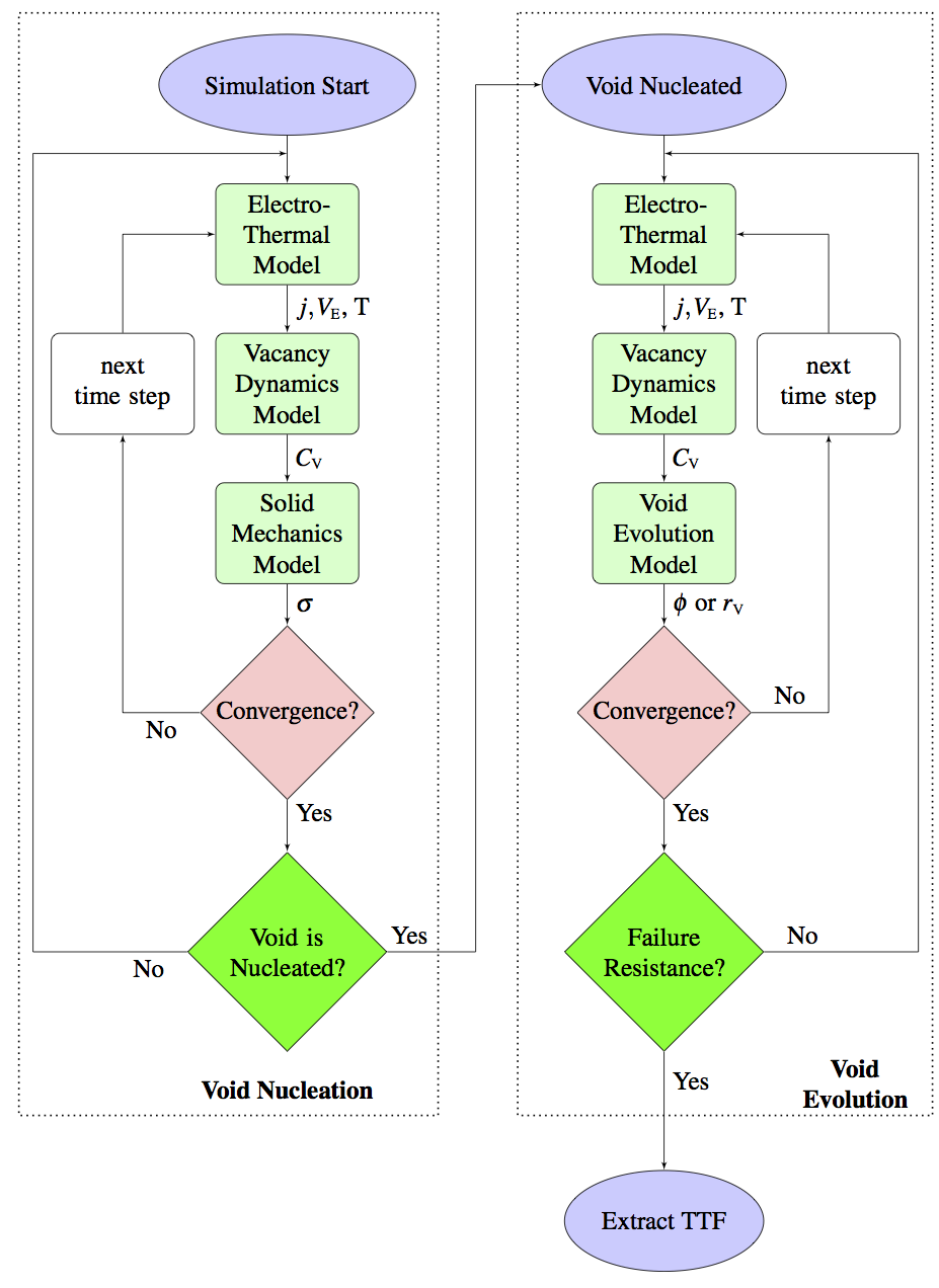
As described in Chapter 1, electromigration induced failure is typically divided in two phases, namely, the early mode of void nucleation and the late mode of void evolution. During the first mode, voids can nucleate at some locations in the interconnect due to stress. This phase lasts until a stable void is nucleated. The time for a void to nucleate is called void nucleation time. The nucleation of a void is the beginning of the late mode, which is governed by the void evolution mechanism. During this phase, the propagation of the void across the interconnect width causes extremely high changes in the interconnect resistance. A morphological change of the void surface at a constant void volume leads to a rapid, non-linear increase in the electrical resistance of the interconnect. The interconnect fails after a maximum tolerable resistance level is reached. The time needed to achieve this maximum resistance is called void evolution time.
Since different physical effects are responsible for each phase of failure development, modeling and simulating electromigration by using FEM-based numerical calculations constitutes a multiphysics analysis which can be divided into the void nucleation phase and the void evolution phase, as depicted in the scheme presented in (4.6). In this way, the complete electromigration time-to-failure (TTF) estimation is obtained by summing the void nucleation time and the void evolution time. The contribution of each component in the electromigration lifetime evaluation depends on different kinetic and physical effects. The modeling of each phase of failure development is necessary for a more precise lifetime prediction and for a better understanding of their impact on the electromigration failure mechanism.
Simulations start with solving the electro-thermal model presented in Section 3.1 in order to obtain the current density j, electric potential Ve, and temperature T distributions in the interconnect from equations (3.3), (3.5), and (3.13) respectively. Then, the vacancy dynamics model, described in Section 3.2, has to be solved in order to determine the distribution of vacancy concentration Cv in the structure. This step is important because it solves the vacancy balance equation (3.26) which takes into account all the various driving forces for vacancy transport (equation (3.24)). The vacancy dynamics problem is followed by the solution of the system of equations (3.58), (3.70) of the solid mechanics model to obtain the stress σ distribution due to electromigration in the interconnect, as presented in Section 3.3. The simulation continues until the threshold stress for void nucleation is reached at some location in the interconnect. Reaching the threshold stress (equation (3.72)) implies void nucleation and the beginning of the second phase of failure development at this location.
Once the void is formed, the void evolution phase begins. In a typical simulation procedure for void evolution, it is convenient to assume an initial small void located at the site of void nucleation. Since the void locally changes the electric current density and vacancy concentration distributions around itself, the electro-thermal and vacancy dynamics analysis have to again be carried out before the evolution is tracked. Then, the void evolution model has to be solved. Depending on the numerical approach, this step of the procedure can be performed in different ways. In Section 3.4, two methodologies are adopted for simulating void evolution in interconnects:
 |
During the simulated void evolution, the resistance of the interconnect can be monitored at each time step. The void evolution procedure is repeated continuously until the resistance of the interconnect increases to a given threshold value which represents the failure criterion. Typically, interconnect failure occurs when a resistance increase of 20% is reached. Subsequently, the lifetime of the interconnect is determined as the time necessary to achieve the maximum tolerable resistance value.